Dr Rajiv Desai
An Educational Blog
The Chip
The Chip:
_
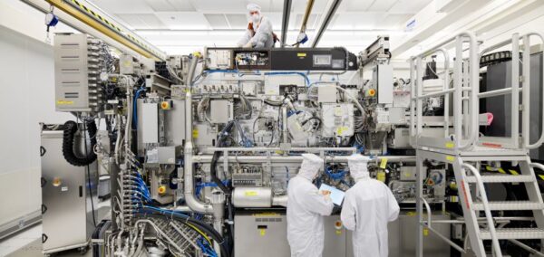
Figure below shows chip manufacturing facility:
______
Section-1
Prologue:
More than 100 years ago, humans invented vacuum tubes that made electricity flow in different directions or get stronger. The tubes made it possible to invent radios, televisions and computers. Every electronic device like a computer and radio works by controlling and manipulating the flow of electric current through a network of interconnected elements like capacitors, diodes and transistors. Before the invention of the chip, electronic devices such as computers and radios used vacuum tubes, or valves, which were cumbersome, heavy and generated a large amount of heat while consuming a lot of power. A 1940s computer called the ENIAC with vacuum tubes about the size of an adult thumb was about the same length and weight as three to four double-decker buses and contained 18,000 vacuum tubes, 7,200 crystal diodes, 1,500 relays, 70,000 resistors, 10,000 capacitors, and approximately 5,000,000 hand-soldered joints. It was big, power-hungry machine that needed its own mini electricity plant to keep it running. This power requirement led to the rumor that whenever the computer was switched on, lights in Philadelphia dimmed.
_
Then transistors were invented. Transistors also help electricity flow, stop, and go. Radios, which used vacuum tubes until then, were significantly downsized and became portable as vacuum tubes were being replaced by the transistor. Transistors are connected to one another or integrated to make circuit. If a circuit is a kind of road where electric signals flow, transistors are a kind of traffic light, or switch. An integrated circuit (IC), sometimes called a chip or microchip, is a semiconductor wafer on which thousands or millions of microscopic transistors, resistors and capacitors are fabricated. The prefix “micro” refers not to the chip itself, although a typical microchip is quite small—a centimeter or less on a side—but to the microscopic components it contains. These microscopic transistors require a substance known as a semiconductor to work – which is why they’re also referred to as semiconductors (chips). Semiconductors are materials that normally don’t conduct electricity (insulators), but can conduct if a small amount of energy is applied. Metals are great because they conduct electricity, but they’re not good for switches because there’s really nothing you can do to turn off that conduction. Semiconductors would be insulators and not conductive at all, which is what makes the ‘off state’, but then if you put in an extra charge, they start conducting. There are a few materials that can be used as semiconductors, and silicon is the substance of choice. The invention of semiconductor devices made it possible to produce solid-state devices, which are smaller, more efficient, reliable, durable, safer, and more economical than vacuum tubes. An IC can function as an amplifier, oscillator, timer, counter, computer memory, or microprocessor.
_
Semiconductors, also known as integrated circuits, computer chips, microchips, or just “chips,” drive the digital economy. Containing thousands of miniature electronic components all connected together, semiconductors are the “brains” of all modern electronics, from consumer products including televisions, laptop computers, tablets, and mobile phones, to more sophisticated equipment used in aerospace, business operations, industrial applications, education, research, communications, healthcare, transportation, energy and national defense. Semiconductors are arguably humanity’s greatest achievement to date. There are chips in nearly everything electric, from phone to computer to car to MRI scanners to industrial robots and data centers. There are even chips in items you wouldn’t expect, such as washing machine, electric toothbrush, and refrigerator. A chip is a collection of anywhere from a few hundred to tens of billions of tiny circuits on a small wafer of silicon. On a chip, silicon transistors are miniature switches that can be turned on and off by electronic signals. These microscopic transistors are like tiny little gates, allowing electrons to pass through them or not. Most of a chip’s integrated circuits contain digital logic functions. Some are analog-only, while others are mixed-mode analog and digital. Digital chips are used for computer processors, memory and other logic and information processing functions. Most chips are groups of circuits that run software, manipulate data and control the functions of electronic devices. The arrangement of those circuits gives them their specific purpose. Chip companies try to pack more transistors into chips, enhancing performance and making devices more power efficient. Intel’s first microprocessor—the 4004—was released in 1971 and contained only 2,300 transistors with a node size of 10 microns, or 10 millionths of a meter. But Intel’s undisputed leadership of the following decades ended between 2015 and 2020 when rivals Taiwan Semiconductor Manufacturing Co. and Samsung Electronics Co. started building chips with better transistors: ones with dimensions down to 5 nanometers, or 5 billionths of a meter (for comparison, an average human hair is 100,000 nanometers wide).
_
Silicon wafer is a thin slice of silicon used for the fabrication of multiple chips. A typical silicon wafer size is 300 mm in diameter and 775 μm in thickness. The process of transforming silicon wafer into tiny microchips or just chips—takes nearly three months. The chip manufacturing factory is known as fab. Semiconductors are astonishing, with billions of transistors packed into a space the size of a dime, and they are astonishingly hard to make. At typical fab, the journey from raw material to finished chip—what engineers call the process flow—is typically 85 days and encompasses more than 300 steps with zero mistakes. The whole time, the chips travel in sealed pods called FOUPs, entirely untouched by human hands. FOUP is an acronym for Front Opening Unified Pod or Front Opening Universal Pod. It is a specialized plastic enclosure designed to hold silicon wafers securely and safely in a controlled environment, and to allow the wafers to be transferred between machines for processing or measurement. The robots do the driving, careening on their suspended tracks above machines the size of small recreational vehicles. One polishes wafers with a slurry that acts like liquid sandpaper. Another uses UV light to imprint circuits just few nanometers wide. Electron microscopes inspect the wafers for imperfections, and a robotic arm immerses them into a chemical bath. Wafers are basically bounced to and from each section of the fab, all day every day. It’s a lot of putting things on, taking it off, printing, putting more on, taking more off, layer by layer. Humans intrude only when something goes wrong. The chips are made in a long and complex process involved using state-of-the art facilities and highly skilled personnel. The construction of modern chips needs very specific expertise and equipment to work, that is why it’s not easy to increase the supply of chips when demand goes up. You can’t just simply start making more. You have to build $10 billion factories in order to make the chips.
_
These chips are the lifeblood of modern society, but even before the pandemic, demand for them exceeded supply. The global chip shortage is due to a combination of different events with the snowball effect of the COVID-19 pandemic being the primary reason for accelerating shortages. The car industry has been hardest hit of all. When the initial lockdowns caused car sales to collapse, automakers cut their orders for parts, including semiconductors. A typical new car can contain more than a thousand chips. Chip manufacturers saw the slack and shifted their output to serve the surging demand for consumer electronics, like webcams and laptops. But when car sales snapped back, a dramatic misstep became apparent: the automakers couldn’t get enough chips. Carmakers slashed production. PlayStations got harder to find in stores. All of these phenomena and more had a similar cause: an abrupt and cascading shortage of semiconductors (integrated circuits or chips). Chips, long revered as the brains of modern society, have become its biggest headache. The stakes extend beyond pandemic-era shortages. Because chips are a crucial component of so many strategic technologies—from renewable energy and artificial intelligence to robots and cybersecurity—their manufacturing has become a geopolitical thorn. In the 20th century, oil was the supreme global resource. But chip shortages have prompted a 21st century catchphrase among policymakers and diplomats: Chips are the new oil. As the world resets to post-pandemic life, a steady supply of semiconductors has become a high-priority benchmark of preparedness and resilience. It will be a year or two before supply can meet demand. While major semiconductor manufacturers such as Taiwan Semiconductor Manufacturing Co, Samsung Electronics Co, and Intel Corp have announced tens of billions of dollars in investments for new factories, the digitalization trend ramped up by the pandemic would continue to drive demand higher. Hundreds of billions of dollars will be spent in the coming years in a global race to expand production, with geopolitical as well as economic implications.
_______
_______
Abbreviations and synonyms:
Si = silicon
SiO2 = silicon dioxide
MOS = metal oxide semiconductor
PMOS = p-type MOS
NMOS = n-type MOS
CMOS = complementary metal oxide semiconductor
FET = field effect transistors
MOSFET = metal oxide semiconductor (silicon) field effect transistors
FinFET = fin field effect transistor
SSI = Small-Scale Integration
MSI = Medium-Scale Integrations
LSI = Large-scale integration
VLSI = Very-large-scale integration
ULSI = Ultra-Large-Scale Integration
TSV = through-silicon via
CAD = Computer-aided design
EDA = Electronic design automation
GVC = Global value chain
IC = Integrated circuit
3D IC = three-dimensional integrated circuit
RISC = Reduced instruction set computing
CISC = Complex instruction set computing
ASIC = Application Specific Integrated Circuit
IDM = Integrated device manufacturer
IOT = Internet of Things
IP = Intellectual property
ODM = Original design manufacturers
PC = Personal computer
SOC = System-on-chip
SOP = System-on-Package
TI = Texas Instruments
TSMC = Taiwan Semiconductor Manufacturing Co.
SMIC = Semiconductor Manufacturing International Corporation
SEMI = Semiconductor Equipment and Materials International
SIA = Semiconductor Industry Association of USA
FOUP = Front Opening Unified Pod = Front Opening Universal Pod
EUVL = extreme ultraviolet lithography
_____
_____
Section-2
Terminology:
Atom: The basic unit of a chemical element. Atoms are made up of a dense nucleus that contains positively charged protons and uncharged neutrons. The nucleus is orbited by a cloud of negatively charged electrons.
Carbon: The chemical element having the atomic number 6. It is the physical basis of all life on Earth. Carbon exists freely as graphite and diamond. It is an important part of coal, limestone and petroleum, and is capable of self-bonding, chemically, to form an enormous number of chemically, biologically and commercially important molecules.
Carbon nanotube: A millionth-of-a-meter scale, tube-shaped material that is made from carbon. It conducts heat and electricity well.
Circuit: A network that transmits electrical signals. In the body, nerve cells create circuits that relay electrical signals to the brain. In electronics, wires typically route those signals to activate some mechanical, computational or other function.
Conductor (in physics and engineering): A material through which an electrical current can flow.
Capacitors and inductors: These are electronic components that can store energy supplied by a voltage source. A capacitor stores energy in an electric field; an inductor stores energy in a magnetic field.
Conductance: It is defined as the potential for a substance to conduct electricity.
Inductance: It is the tendency of an electrical conductor to oppose a change in the electric current flowing through it by generating a self-induced emf within itself as a result of their changing magnetic field.
Current (in electricity): The flow of electricity or the amount of charge moving through some material over a particular period of time.
Data: For digital information (the type stored by computers), those data typically are numbers stored in a binary code, portrayed as strings of zeros and ones.
Digital (in computer science and engineering): An adjective indicating that something has been developed numerically on a computer or on some other electronic device, based on a binary system (where all numbers are displayed using a series of only zeros and ones).
Electricity: It is transfer of electrical energy as electromagnetic waves from source to load using motion of charged particles (electrons in copper wire) as source of photons under influence of voltage.
Electronics: It is a branch of physics and electrical engineering that deals with the emission, behavior, and effects of electrons (as in electron tubes and transistors) and with electronic devices. It involves devices that are powered by electricity but whose properties are controlled by the semiconductors or other circuitry that channel or gate the movement of electric charges.
Insulator: A substance or device that does not readily conduct electricity.
Micrometer (sometimes called a micron): One thousandth of a millimeter, or one millionth of a meter.
Nanometer (nm): Unit of measure (one billionth of a meter); used in reference to a process technology’s minimum feature size (e.g., ‘7nm process technology’)
Semiconductor: A material that sometimes conducts electricity. Semiconductors are important parts of computer chips and certain new electronic technologies, such as light-emitting diodes.
Silicon: A nonmetal, semiconducting element used in making electronic circuits. Pure silicon exists in a shiny, dark-gray crystalline form and as a shapeless powder.
Silicone: A silicone is a polymer made up of siloxane. They are typically colorless oils or rubber-like substances. Silicones are used in sealants, adhesives, lubricants, medicine, cooking utensils, thermal insulation, and electrical insulation. Silicones consist of an inorganic silicon–oxygen backbone chain (⋯−Si−O−Si−O−Si−O−⋯) with two organic groups attached to each silicon center. Commonly, the organic groups are methyl.
Central Processing Unit (CPU): The main control circuit of a computer that carries out arithmetic, logic, control and input/output (I/O) operations, it is also called processor.
Chiplet: An integrated circuit (IC) that contains a subset of the functional blocks typically required for a full System-On-Chip (SOC)
Die: A small block of semiconducting material on which a specific functional IC is made
Fabless Business Model: A leading business model in the semiconductor industry allowing companies to direct more profits toward research and development and growth strategies
Graphics Processing Unit (GPU): Circuits that perform simultaneous operations of large amounts of data for creation of images on a display or non-graphic computations such as machine learning analyses
Integrated Circuit (IC): A set of electronic circuits designed onto one small area of a semiconductor material (such as silicon)
Original Equipment Manufacturer (OEM): Company that assembles or produces final end-user devices to be marketed or sold by it or by others
Package: A metal, plastic, glass, or ceramic casing containing one or more discrete ICs
Process technology: The specific design rules and manufacturing process for a semiconductor; also known as technology node, process node, or just node
System-on-Chip (SOC): An IC that combines many components of a computer or other electronic system on the same chip
Transistor: A component that can act like a switch for electrical signals i.e., regulates the flow of electrical current, and is a building block for ICs
Wafer: A thin slice of silicon used for the fabrication of multiple ICs
_____
_____
What is Semiconductor?
A semiconductor material has an electrical conductivity value falling between that of a conductor, such as metallic copper, and an insulator, such as glass. Its resistivity falls as its temperature rises; metals behave in the opposite way. ICs (integrated circuits) and electronic discrete components such as diodes and transistors are made of semiconductors. Semiconductor refers to a material whose conductivity can be controlled, ranging from insulators to conductors. Common elemental semiconductors are silicon and germanium. Silicon is well-known of these. Silicon forms most of ICs.
What is IC?
An integrated circuit (IC) is defined as:
A circuit in which all or some of the circuit elements are inseparably associated and electrically interconnected so that it is considered to be indivisible for the purposes of construction and commerce. Circuits meeting this definition can be constructed using many different technologies, including thin-film transistors, thick-film technologies, or hybrid integrated circuits. However, in general usage integrated circuit has come to refer to the single-piece circuit construction originally known as a monolithic integrated circuit, often built on a single piece of silicon.
A semiconductor integrated circuit is a combination of active components such as transistors, diodes, and passive components such as resistors and capacitors, which are interconnected according to a certain circuit and “integrated” on a single semiconductor chip to complete a specific circuit or system function. It is through the semiconductor manufacturing processes of oxidation, photolithography, diffusion, epitaxy, and aluminum evaporation, the semiconductor, resistor, capacitor and other components required to form a circuit with a certain function and the connecting wires between them are all integrated into a small piece of silicon on-chip, then solder the electronic devices packaged in a package.
What is Chip?
Chip is the general term for semiconductor component products. Chip is another name for the IC, or you can say a chip is the carrier of the IC. A silicon chip is a very small piece of silicon containing integrated circuits. Silicon wafer is divided in to multiple chips. A chip is manufactured from a silicon wafer, which is first cut to size and then etched with circuits and electronic devices. The electronic devices use complementary metal-oxide semiconductor (CMOS) technology. The current stage of micro-integration is known as Ultra Large-Scale Integration (VLSI). Chip is short for microchip, the incredibly complex yet tiny modules that store computer memory or provide logic circuitry for microprocessors. Many special-purpose chips, known as application-specific integrated circuits, are being made today for automobiles, home appliances, telephones, and other devices.
What is the difference between a chip and a processor?
A chip of silicon (any semiconductor) can have amplifiers, logic blocks, line drivers and receivers, cell phone transmitters and receivers, phase lock loops, audio and RF functions and even light emitting structures. A chip of silicon can have only memory on it with no processing power. So a processor is only one of many functions possible on a chip. Not all chips are processors. A chip has become a generic term for an integrated circuit. This can include modems, memory modules, and other types of integrated circuits that are not typically considered processors. All processors are chips but all chips are not processors. The different types of processors are microprocessor, microcontroller, embedded processor, digital signal processor and the processors can be varied according to the devices.
What is Wafer?
A wafer is the base of an IC. Wafers are made of silicon. When silicon is purified and melted into the liquid, manufacturers pull it into a crystal column. On the silicon crystal column, there are the crystal lattices in a specific arrangement that the manufacturer designs. Then manufacturers cut the crystal column into thin slices using a diamond knife. After polishing, these slices become wafers. In electronics, a wafer is known as a slice or substrate. It is a thin slice of [Wafer] semiconductor material and this slice is used for the fabrication of integrated circuits. It acts like a base on which an integrated circuit can be formed. The microcircuits on the wafers are constructed by the diffusion and deposition of various substances. The difference between a wafer and a chip resides in the relation between them. A wafer acts as a base for chip or chip is embedded in the wafer. From a 300mm size silicon wafer, 263 chips (ICs) of size 16mm X 16 mm can be made. A die is a small block of semiconducting material on which a given functional circuit is fabricated. Die is an unpackaged, bare chip. A die is the formal term for the square of silicon containing an integrated circuit that has been cut out of the wafer. Typically, identical integrated circuits are produced in large batches on a single wafer of electronic-grade silicon through processes such as photolithography.
Note:
The terms ‘die’ ‘chip’ and ‘IC’ are used interchangeably although there is very subtle difference among them.
What is an RF semiconductor?
“RF” refers to the use of electromagnetic radiation for transferring information between two circuits that have no direct electrical connection. Time-varying voltages and currents generate electromagnetic energy that propagates in the form of waves. RF semiconductors are used in the telecommunication, aerospace, automotive, and defense fields. RF semiconductors work in a radio frequency spectrum of about 3KHz up to 300GHz.
What is a semiconductor optical amplifier?
A semiconductor optical amplifier is an optical amplifier based on a semiconductor gain medium. The semiconductor optical amplifier is of small size, electrically pumped and can be integrated with semiconductor lasers, modulators, etc. Users can find SOAs in optical transceiver modules used to enable communication between data centers. In this scenario, the SOA amplifies the optical signal used for Ethernet communication. This approach helps compensate for transmission loss.
What is a fabless chip maker?
The term “fabless” means that the company designs and sells the hardware and semiconductor chips but does not manufacture the silicon wafers, or chips, used in its products; instead, it outsources the fabrication to a manufacturing plant or foundry.
______
______
Section-3
Introduction to microchip/chip/IC:
A microchip is a small semiconductor used to relay information via specific electrical characteristics. Microchips—also called silicon chips, integrated circuits, and several other terms—are small, thin, rectangular chips or tiles of a crystalline semiconductor, usually silicon, that have been layered with large numbers of microscopic transistors and other electronic devices. These devices are a part of the chip’s crystal structure, that is, integral to it—hence the term “integrated circuit.” An integrated circuit may contain billions of individual devices but is one solid object. It starts with growing and purifying silicon, slicing wafers of the silicon material, photo etching circuit designs on them composed of mainly transistors, resistors, capacitors, and inductors; then packaging it with pins so it can be mounted and soldered on a circuit card. An integrated circuit is used as a controller switch to perform a specific task. The transistor in the integrated circuit acts like an on and off switch. The resistor controls the electrical current that moves back and forth between the transistors. The capacitor collects and releases electricity, while a diode stops the flow of electricity.
The prefix “micro” refers not to the chip itself, although a typical microchip is quite small—a centimeter or less on a side—but to the microscopic components it contains. The microchip has made it possible to miniaturize computers, communications devices, controllers, and hundreds of other devices. Since 1971, whole computer CPUs (central processing units) have been placed on microchips. These affordable, highly complex devices—microprocessors—have been the basis of the computer revolution. By 2008, at least 5 billion microchips were being manufactured every year in the United States alone, and many more were being manufactured globally. Microchips and computers are now used in scientific instruments, military weapons, personal entertainment devices, communications devices, vehicles, computers, and many other applications, and are an important part of the global economy. In 2007, the global semiconductor industry sold about $256 billion worth of microchips. The social effects of cheap computation have been profound, though not as overwhelming as computer enthusiasts have repeatedly predicted.
_
An integrated circuit (ICs) is an electronic device comprising numerous functional elements such as transistors, resistors, condensers, etc. on a piece of silicon semiconductor substrate, and is sealed inside a package with multiple terminals. The basic idea is to take a complete circuit, with all its many components and the connections between them, and recreate the whole thing in microscopically tiny form on the surface of a piece of silicon. At present, IC critical dimensions (or smallest dimensions of IC elements) are in the order of 10 nanometers, which is extremely small. Transistor radios that fascinated boys in the old days consisted of a piece of printed board with discrete transistors, resistors, condensers and diodes inserted, which were wired to each other. The current IC is highly integrated and miniaturized, about 1/55000 of the size and 3 billionths of the area of the transistor radio. Owing to their high integration, ICs with various functions embedded have dramatically enhanced the performance of electronics.
_
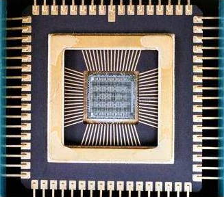
Figure below shows an integrated circuit from the inside. The integrated circuit is the tiny square in the center. Connections (wires) run out from it to the terminals (metal pins or legs) around the edge. When you hook up something to one of these terminals, you’re actually connecting into the circuit itself. You can just about see the pattern of electronic components on the surface of the chip itself.
There are several basic classifications of chips, including analog, digital and mixed signal varieties. These different classifications of chips determine how they transmit signals and handle power. Their size and efficiency are also dependent upon their classification, and the digital chip is the smallest, most efficient, most powerful and most widely used, transmitting data signals as a combination of ones and zeros.
_
In the manufacturing of ICs, many identical ICs are made on a silicon wafer and then cut (diced) into numerous IC chips (dies). The IC chips are sealed inside packages because they are too small to be electrically bonded to a printed circuit board, and also because IC chips would get broken if left unprotected.
If you open the cover of a personal computer, you will see objects with multiple legs (pins) sticking out. These are the ICs hidden inside the packages.
All the IC’s have interconnected discreet devices inside the chip and the corresponding external connecting terminals outside. Each pin may have distinct function and may vary according to the manufacturer’s design. In order to make the circuit fully operative, the pins in the IC must be used for supply voltage, input and output connections, and also some external components according to the needs of the manufacturer.
Chip Packages:
Chips come various packages or styles. These include single in-line packages (SIPs), which have one straight line of legs; pin-grid arrays (PGAs), which have pins arranged in concentric squares; and dual in-line packages (DIPs), which have between eight and 40 legs, divided evenly between two rows. Other chip styles include PLCC (Plastic leaded chip carrier), TSOP (Thin small-outline package), and PQFP (Plastic Quad Flat Pack).
Chips can also come as part of a single in-line memory module, or SIMM, which is comprised of up to nine chips, compressed into a single unit.
_
An integrated circuit (more often called an IC, microchip, silicon chip, computer chip, or chip) is a piece of specially prepared silicon (or another semiconductor) into which a very complex electronic circuit is etched using photographic techniques. Silicon chips can contain computer processors, memory and special devices. The chip is very fragile and so is normally surrounded by a tough plastic package, and electrical contact with the chip is provided through metal legs sticking out of the package. ICs are designed for different purposes. A chip may be designed as a calculator, which only works as a calculator. Integrated circuits can be classified into analog, digital and mixed signal (both analog and digital on the same chip). A semiconductor such as silicon can be controlled to conduct much or little. This allows making transistors that control each other. They are found in many household items such as radio, computers, telephones and other devices. Other semiconductor devices include solar cells, diodes, and LED’s (light emitting diode).
_
The body of most chips is made of silicon. This material is used because it is a semiconductor. In its pure form, silicon does not conduct electricity at room temperature. But if certain impurities are added to silicon, it can carry an electric current. Manufacturers ‘dope’ silicon chips with such impurities as boron and phosphorus. The doped regions form the chip’s electronic components, which control the electric signals carried on the chip. The type and arrangement of the impurities determine how each component controls signals. Most components serve as switches called transistors. Others serve mainly as capacitors, which store an electric charge; diodes, which prevent current from flowing in one direction but not the other, and resistors, which control voltage.
_
There are a number of different ways to build a microchip. How it is built depends on the chip’s intended use. In the case of a personal computer, the main ingredient for most chips is silicon. The manufacturing of a computer chip begins with a wafer of doped silicon. The wafer measures from 2.5 to 30 centimeters in diameter. A photographic process reduces a large master design for the integrated circuit to microscopic size. Technicians use these microscopic designs, called masks, as stencils to make hundreds of chips on one wafer. The actual circuit design is drawn onto the chip using ultraviolet light with a stencil, or mask, as a guide. Afterwards, wiring and transistor components are built onto the design. Complex integrated circuits can have multiple layers of built-in, interconnected components. Chip manufacturers add other metals, such as aluminum, copper and gold, to enhance the chip’s capabilities. The data storage and manipulation capabilities of microchips are performed by built-in transistor components. The electric current is translated into useable data by sending the current through the circuit in a series of charges. The charges actually become the language needed to communicate with a receiving device. Boolean logic is the language used to translate electrical currents into useable instructions for a computer. In its simplest form, Boolean logic is a binary code that uses two values–true and false, or “on and off”–to translate electrical current into a useable message. After the wafer has been processed, it is divided into individual chips. Some chips contain millions of components. Manufacturers create thin lines of metal – usually aluminium – on the chip to connect these tiny components.
_
The transistors inside chip can be bipolar transistors in unusual circuits, such as those needing very high switching speeds. Most, however, are MOSFETs. Nearly all modern IC chips are metal–oxide–semiconductor (MOS) integrated circuits, built from MOSFETs (metal–oxide–silicon field-effect transistors). As of 2018, the vast majority of all transistors are MOSFETs fabricated in a single layer on one side of a chip of silicon in a flat two-dimensional planar process. Researchers have produced prototypes of several promising alternatives, such as:
-1. various approaches to stacking several layers of transistors to make a three-dimensional integrated circuit (3DIC), such as through-silicon via, monolithic 3D, stacked wire bonding, and other methodologies.
-2. transistors built from other materials: graphene transistors, molybdenite transistors, carbon nanotube field-effect transistor, gallium nitride transistor, transistor-like nanowire electronic devices, organic field-effect transistor, etc.
-3. fabricating transistors over the entire surface of a small sphere of silicon.
-4. modifications to the substrate, typically to make “flexible transistors” for flexible display or other flexible electronics, possibly leading to a roll-away computer.
_
Feature Size measured in Nanometers:
The size of the features (the elements that make up the structures on a chip) are measured in nanometers. A 22 nm process technology refers to features 22 nm or 0.022 µm in size. Historically, the feature size referred to the length of the silicon channel between source and drain in field effect transistors (FET). Today, Feature size is either the minimum distance between the source and drain on a MOS transistor or half the distance between cells in a dynamic RAM chip (known as “DRAM half pitch”). Certain elements within the transistor may even be smaller than the published feature size for a technology generation. The feature size of the 486 chip in 1989 was 1,000 nm (one micron). By 2003, it was 90 nm, reduced by a little less than one millionth of a meter. What may seem a minuscule reduction took a massive amount of money and R&D. At any given time, the smallest feature sizes are found on the latest, high-end CPU and SoC chips that cost several hundred dollars. However, 8-bit and 16-bit microcontrollers (MCUs) are used by the billions and sell for as little as 50 cents in quantity. They require far fewer transistors and do not need to be as dense. A $2 microcontroller may have feature sizes similar to the high-end chips a decade or two earlier.
The technology node (also process node, process technology or simply node) refers to a specific semiconductor manufacturing process and its design rules. Different nodes often imply different circuit generations and architectures. Generally, the smaller the technology node means the smaller the feature size, producing smaller transistors which are both faster and more power-efficient. Historically, the process node name referred to a number of different features of a transistor including the gate length as well as M1 half-pitch. The half-pitch refers to half the minimum center-to-center distance spacing (or pitch) between Metal 1 lines. Most recently, due to various marketing and discrepancies among foundries, the number itself has lost the exact meaning it once held. Since 2009, “node” has become a commercial name for marketing purposes that indicates new generations of process technologies, without any relation to gate length, metal pitch or gate pitch. For example, GlobalFoundries’ 7 nm process is similar to Intel’s 10 nm process, thus the conventional notion of a process node has become blurred. Additionally, TSMC and Samsung’s 10 nm processes are only slightly denser than Intel’s 14 nm in transistor density. They are actually much closer to Intel’s 14 nm process than they are to Intel’s 10 nm process (e.g., Samsung’s 10 nm processes’ fin pitch is the exact same as that of Intel’s 14 nm process: 42 nm).
_
MOSFET scaling:
(Process nodes)
10 µm – 1971
6 µm – 1974
3 µm – 1977
1.5 µm – 1981
1 µm – 1984
800 nm – 1987
600 nm – 1990
350 nm – 1993
250 nm – 1996
180 nm – 1999
130 nm – 2001
90 nm – 2003
65 nm – 2005
45 nm – 2007
32 nm – 2009
22 nm – 2012
14 nm – 2014
10 nm – 2016
7 nm – 2018
5 nm – 2020
Future:
3 nm ~ 2022
2 nm ~ 2024
1.8 nm ~ 2025
_
Integrated circuits have their origin in the invention of the transistor in 1947 by William B. Shockley and his team at the American Telephone and Telegraph Company’s Bell Laboratories. Shockley’s team (including John Bardeen and Walter H. Brattain) found that, under the right circumstances, electrons would form a barrier at the surface of certain crystals, and they learned to control the flow of electricity through the crystal by manipulating this barrier. Controlling electron flow through a crystal allowed the team to create a device that could perform certain electrical operations, such as signal amplification, that were previously done by vacuum tubes. They named this device a transistor, from a combination of the words transfer and resistor. The study of methods of creating electronic devices using solid materials became known as solid-state electronics. Solid-state devices proved to be much sturdier, easier to work with, more reliable, much smaller, and less expensive than vacuum tubes. Using the same principles and materials, engineers soon learned to create other electrical components, such as resistors and capacitors. Now that electrical devices could be made so small, the largest part of a circuit was the awkward wiring between the devices.
In 1958 Jack Kilby of Texas Instruments, Inc., and Robert Noyce of Fairchild Semiconductor Corporation independently thought of a way to reduce circuit size further. They laid very thin paths of metal (usually aluminum or copper) directly on the same piece of material as their devices. These small paths acted as wires. With this technique an entire circuit could be “integrated” on a single piece of solid material and an integrated circuit (IC) thus created. Today, integrated circuits, or ICs, are small pieces of flat silicon that can be as small as a few square millimeters. Individual circuit components are generally microscopic. Different circuit elements are thin substrates of semiconductors arranged in permanent patterns. Different arrangements result in various miniaturized devices like transistors, gates, diodes, capacitors, and resistors. The assembly of tiny switches is engineered to process input signals into predictable outputs. The IC’s mass production capability, reliability, and building-block approach to integrated circuit design has ensured the rapid adoption of standardized ICs in place of designs using discrete transistors. ICs are now used in virtually all electronic equipment and have revolutionized the world of electronics. Computers, mobile phones, and other digital home appliances are now inextricable parts of the structure of modern societies, made possible by the small size and low cost of ICs such as modern computer processors and microcontrollers.
_
Furthermore, it is important to know how microchips are made. The beginning process of how microchips, also known as integrated circuits, are made, starts with growing a single crystal of silicon or another semiconducting material. After the silicon is melted, it is spun and a seed crystal is put into it. When the silicon begins to cool, the seed crystal gets withdrawn very slowly. The single crystal then gets cut into figures shaped like discs. Each disc is about four to twelve inches across. One side of each wafer is then polished and processed to make lots of identical microchips. Then, the wafers get buffed twice and they are ready for engraving with a circuit design at this point in the process. After that, they get packed with billions of transistors and cut apart. Next, the computer chips get placed into protective packages. Finally, the microchips get joined electrically to the world by metal pins poking out of the tiny packages. Knowing how to make a microchip will help people understand the importance of them.
_
Also, knowing how microchips work is necessary to know how important microchips are. Microchips, or integrated circuits (IC), are basically miniature circuit boards on slices of semiconductor, such as silicon or germanium. These semiconductors can either conduct or insulate electricity when mixed with other elements. For example, silicon conducts electricity when it is mixed with antimony. However, when mixed with boron it will conduct electricity the other way. ICs use this characteristic to create and send instructions to a receiver which will carry them out. ICs usually contain resistors, transistors, diodes, and capacitors. These components form a series of logic gates. These logic gates conduct depending on the electricity input. There are five types of logic gates. One is AND, which conducts electricity when both inputs are one in binary. Second is OR, which becomes one when one of the two inputs are one. The third, NOT, converts zero to one and one to zero. Fourth is NAND, which is basically AND and NOT together. So, if both inputs to AND are one, the NOT will change the one to zero after it goes through AND. The fifth and final gate is NOR. Similar to NAND, NOR is OR and NOT together. A standard cell is a group of transistor and interconnect structures that provides a Boolean logic function (e.g., AND, OR, XOR, XNOR, inverters) or a storage function (flipflop or latch). The simplest cells are direct representations of the elemental NAND, NOR, and XOR Boolean function, although cells of much greater complexity are commonly used (such as a 2-bit full-adder, or muxed D-input flipflop.) By using the logic gates to process inputs, an IC can string together an instruction and send it to the receiver to be followed. An IC does not necessarily need to perform this job, though. A circuitry board with transistors, resistors, and the other components can be used to build instructions. However, ICs can fit the whole circuit into a small space, which can be fitted into small gadgets such as iPods, cell phones, or portable devices. Without microchips, portable devices would not be possible.
_
The invention of the integrated circuit is considered by many experts as one of the most significant innovations in contemporary history. After all, most modern products use chip technology nowadays, including everything from your iPhone to the web hosting services which power this very website. Microchips power most consumer electronic computing devices like the iWatch and iPhone. Microchips are manufactured from germanium and silicon. They are used for the logic component of a computer system, typically called a microprocessor. They’re also used for the computer’s memory, which is called a RAM chip. The integrated circuit works as a control switch and performs a specific action. A transistor in the circuit works like an on and off switch.
Evolution of the microchip microprocessor from invention until today is depicted in figure below.
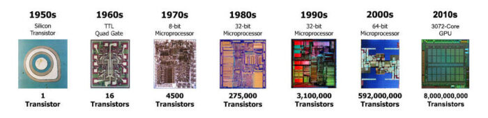
Integrated circuits mean that electronics keep getting smaller. Within a decade of the invention of transistors, engineers called putting dozens of components on chips Small-Scale Integration (SSI). Medium-Scale Integrations (MSI) soon followed adding even more per square centimeter. Today, we have Ultra Large Scale Integration (ULSI) with millions of elements on a single tiny wafer. The number of components on a chip has doubled every year. This phenomenon is named after Gordon Moore, an Intel engineer that first noticed the trend back in the 1960s.
_
There are two major types of computer microchips: Logic chips and Memory chips. The circuitry of microchips determines what they can be used for. The first is called a microprocessor, which carries out the instructions that make up computer programs, and the other type is called a memory chip, which holds computer programs and other data. Logic chips are the ‘brains’ of electronic devices – they process information to complete a task. Among Logic chips, CPUs (central processing units) are the ‘original’ chips, first designed in the 1960s. But there are also processors with specific functionality in mind, such as GPUs (graphical processing units, which are optimized for visual display) and NPUs (neural processing units, designed for deep and machine learning applications).
Memory chips are used primarily in computers. Memory chips store information. A single chip can hold millions of bits; bits are usually grouped into packs of eight called bytes. A letter or symbol can take from one to ten bytes of memory. Memory chips are used for primary storage that can be accessed immediately by the microprocessors. On the other hand, secondary memory storage is not able to be accessed immediately but is stored on a hard disk, DVD, or flash drive. Memory chips are mostly used in computers.
A memory chip is an integrated circuit made out of millions of capacitors and transistors that can store data or can be used to process code. Memory chips can hold memory either temporarily through random access memory (RAM), or permanently through read only memory (ROM). Read only memory contains permanently stored data that a processor can read but cannot modify. Memory chips comes in different sizes and shapes. Some can be connected directly while some need special drives. Memory chips are essential components in computer and electronic devices in which memory storage plays a key role.
_
There are two main types of memory chips: random-access memory (RAM) and read only memory (ROM). RAM is also known as internal memory or main memory. RAM can be easily changed, but it only stores memory as long as the computer is on. There are two different kinds of RAM: static RAM (SRAM) and dynamic RAM (DRAM). DRAM is the majority of a personal computer’s (PC) memory, but DRAM only holds memory for a few thousandths of a second and must be refreshed to hold any information. To refresh DRAM, the computer removes information from a group of cells and then puts the same information back. Cells are memory storage units. DRAM may appear wasteful, but it is cheap to make and it stores a lot of information in a small space. The other type of RAM, SRAM holds memory until a microprocessor changes it.
The other type of memory chip, ROM, retains stored memory even when the computer is off. The user cannot usually change the stored memory. Flash memory, erasable ROM, is ROM that can be reprogrammed, but does not lose information when the computer is turned off. Electrically Erasable and Programmable ROM (EEPROM) can be erased with an electric pulse. Computer programmers can erase and reprogram parts of the microchip. Memory chips are important to microchips because they store the information of the world.
______
______
IC generations:
The driving force behind the design of integrated circuits is miniaturization, and process technology boils down to the never-ending goal of smaller. It means more computing power per square inch and chips that can be placed into ever tighter quarters. In the early days of simple integrated circuits, the technology’s large scale limited each chip to only a few transistors, and the low degree of integration meant the design process was relatively simple. Manufacturing yields were also quite low by today’s standards. As metal–oxide–semiconductor (MOS) technology progressed, millions and then billions of MOS transistors could be placed on one chip, and good designs required thorough planning, giving rise to the field of electronic design automation, or EDA. Some SSI and MSI chips, like discrete transistors, are still mass-produced, both to maintain old equipment and build new devices that require only a few gates. The 7400 series of TTL chips, for example, has become a de facto standard and remains in production.
|
Acronym |
Name |
Year |
Transistor count |
Logic gates number |
|
SSI |
small-scale integration |
1964 |
1 to 10 |
1 to 12 |
|
MSI |
medium-scale integration |
1968 |
10 to 500 |
13 to 99 |
|
LSI |
large-scale integration |
1971 |
500 to 20000 |
100 to 9999 |
|
VLSI |
very large-scale integration |
1980 |
20000 to 1000000 |
10000 to 99999 |
|
ULSI |
ultra-large-scale integration |
1984 |
1000000 and more |
100000 and more |
_
Small-scale integration (SSI)
The first integrated circuits contained only a few transistors. Early digital circuits containing tens of transistors provided a few logic gates, and early linear ICs such as the Plessey SL201 or the Philips TAA320 had as few as two transistors. The number of transistors in an integrated circuit has increased dramatically since then. The term “large scale integration” (LSI) was first used by IBM scientist Rolf Landauer when describing the theoretical concept; that term gave rise to the terms “small-scale integration” (SSI), “medium-scale integration” (MSI), “very-large-scale integration” (VLSI), and “ultra-large-scale integration” (ULSI). The early integrated circuits were SSI.
SSI circuits were crucial to early aerospace projects, and aerospace projects helped inspire development of the technology. Both the Minuteman missile and Apollo program needed lightweight digital computers for their inertial guidance systems. Although the Apollo Guidance Computer led and motivated integrated-circuit technology, it was the Minuteman missile that forced it into mass-production. The Minuteman missile program and various other United States Navy programs accounted for the total $4 million integrated circuit market in 1962, and by 1968, U.S. Government spending on space and defense still accounted for 37% of the $312 million total production.
The demand by the U.S. Government supported the nascent integrated circuit market until costs fell enough to allow IC firms to penetrate the industrial market and eventually the consumer market. The average price per integrated circuit dropped from $50.00 in 1962 to $2.33 in 1968. Integrated circuits began to appear in consumer products by the turn of the 1970s decade. A typical application was FM inter-carrier sound processing in television receivers.
The first application MOS chips were small-scale integration (SSI) chips. Following Mohamed M. Atalla’s proposal of the MOS integrated circuit chip in 1960, the earliest experimental MOS chip to be fabricated was a 16-transistor chip built by Fred Heiman and Steven Hofstein at RCA in 1962. The first practical application of MOS SSI chips was for NASA satellites.
_
Medium-scale integration (MSI)
The next step in the development of integrated circuits introduced devices which contained hundreds of transistors on each chip, called “medium-scale integration” (MSI).
MOSFET scaling technology made it possible to build high-density chips. By 1964, MOS chips had reached higher transistor density and lower manufacturing costs than bipolar chips.
In 1964, Frank Wanlass demonstrated a single-chip 16-bit shift register he designed, with a then-incredible 120 MOS transistors on a single chip. The same year, General Microelectronics introduced the first commercial MOS integrated circuit chip, consisting of 120 p-channel MOS transistors. It was a 20-bit shift register, developed by Robert Norman and Frank Wanlass. MOS chips further increased in complexity at a rate predicted by Moore’s law, leading to chips with hundreds of MOSFETs on a chip by the late 1960s.
_
Large-scale integration (LSI)
Further development, driven by the same MOSFET scaling technology and economic factors, led to “large-scale integration” (LSI) by the mid-1970s, with tens of thousands of transistors per chip.
The masks used to process and manufacture SSI, MSI and early LSI and VLSI devices (such as the microprocessors of the early 1970s) were mostly created by hand, often using Rubylith-tape or similar. For large or complex ICs (such as memories or processors), this was often done by specially hired professionals in charge of circuit layout, placed under the supervision of a team of engineers, who would also, along with the circuit designers, inspect and verify the correctness and completeness of each mask.
Integrated circuits such as 1K-bit RAMs, calculator chips, and the first microprocessors, that began to be manufactured in moderate quantities in the early 1970s, had under 4,000 transistors. True LSI circuits, approaching 10,000 transistors, began to be produced around 1974, for computer main memories and second-generation microprocessors.
_
Very-large-scale integration (VLSI)
“Very-large-scale integration” (VLSI) is a development started with hundreds of thousands of transistors in the early 1980s, and, as of 2016, transistor counts continue to grow beyond ten billion transistors per chip.
Multiple developments were required to achieve this increased density. Manufacturers moved to smaller MOSFET design rules and cleaner fabrication facilities. The path of process improvements was summarized by the International Technology Roadmap for Semiconductors (ITRS), which has since been succeeded by the International Roadmap for Devices and Systems (IRDS). Electronic design tools improved, making it practical to finish designs in a reasonable time. The more energy-efficient CMOS replaced NMOS and PMOS, avoiding a prohibitive increase in power consumption. The complexity and density of modern VLSI devices made it no longer feasible to check the masks or do the original design by hand. Instead, engineers use EDA tools to perform most functional verification work. Electronic design automation (EDA), also referred to as electronic computer-aided design (ECAD), is a category of software tools for designing electronic systems such as integrated circuits and printed circuit boards. The tools work together in a design flow that chip designers use to design and analyze entire semiconductor chips. Since a modern semiconductor chip can have billions of components, EDA tools are essential for their design.
In 1986, one-megabit random-access memory (RAM) chips were introduced, containing more than one million transistors. Microprocessor chips passed the million-transistor mark in 1989 and the billion-transistor mark in 2005. The trend continues largely unabated, with chips introduced in 2007 containing tens of billions of memory transistors.
_
ULSI, WSI, SoC and 3D-IC:
-To reflect further growth of the complexity, the term ULSI that stands for “ultra-large-scale integration” was proposed for chips of more than 1 million transistors.
-Wafer-scale integration (WSI) is a means of building very large integrated circuits that uses an entire silicon wafer to produce a single “super-chip”. Through a combination of large size and reduced packaging, WSI could lead to dramatically reduced costs for some systems, notably massively parallel supercomputers. The name is taken from the term Very-Large-Scale Integration, the current state of the art when WSI was being developed.
-A system-on-a-chip (SoC or SOC) is an integrated circuit in which all the components needed for a computer or other system are included on a single chip. The design of such a device can be complex and costly, and whilst performance benefits can be had from integrating all needed components on one die, the cost of licensing and developing a one-die machine still outweigh having separate devices. With appropriate licensing, these drawbacks are offset by lower manufacturing and assembly costs and by a greatly reduced power budget: because signals among the components are kept on-die, much less power is required. Further, signal sources and destinations are physically closer on die, reducing the length of wiring and therefore latency, transmission power costs and waste heat from communication between modules on the same chip. This has led to an exploration of so-called Network-on-Chip (NoC) devices, which apply system-on-chip design methodologies to digital communication networks as opposed to traditional bus architectures.
______
______
3D IC:
In a 2D chip, the vast majority of all transistors are MOSFETs fabricated in a single layer on one side of a chip of silicon in a flat two-dimensional planar process. In traditional 2D electronic circuits, each die is packaged separately. The packaged chips are laid out on a circuit board and connected to one another with tiny wires.
In the world of semiconductors and microelectronics, a trend to vertically stack integrated circuits (ICs) or circuitry has emerged as a viable solution for meeting electronic device requirements such as higher performance, increased functionality, lower power consumption, and a smaller footprint. The various methods and processes used to achieve this are called 3D integration technologies.
3D ICs are integrated circuits (chips) that incorporate two or more layers of circuitry in a single package. The layers are interconnected vertically as well as horizontally. These multi-layer chips are usually created by manufacturing separate layers and then stacking and thinning them. Vertical electrical connections – TSVs – pierce the underlying silicon substrates to connect the circuitry on the different layers. Stacking can be done die-on-die, die-on-wafer, wafer-on-wafer, or in combination. The thickness of the layers, the diameter of the TSVs, and the number and density of the TSVs are important factors in the performance of the finished 3D IC. The classic definition that has emerged for 3D ICs is logic on logic, connected with through-silicon vias (TSVs). But there are other iterations of this idea, ranging from package-on-package (PoP), homogeneous memory stacks on logic, and hybrid chips that combine some elements of 2.5D with 3D memory and almost-3D memory. There are even some new approaches being presented, including wireless connectivity between very thin die, and wafer-level packaging rather than die-on-die packaging.
The 3D IC is one of several 3D integration schemes that exploit the z-direction to achieve electrical performance benefits in microelectronics and nanoelectronics. In general, 3D integration is a broad term that includes such technologies as 3D wafer-level packaging; 2.5D and 3D interposer-based integration; 3D stacked ICs (3D-SICs), monolithic 3D ICs; 3D heterogeneous integration; and 3D systems integration.
3D integrated circuits can be classified by their level of interconnect hierarchy at the global (package), intermediate (bond pad) and local (transistor) level. 3D ICs can be divided into 3D Stacked ICs (3D-SICs), which refers to stacking IC chips and interconnecting them with TSVs; and true 3D ICs, which use fab processes to stack multiple device layers on a single chip, which may or may not use very-fine-pitch TSVs to form the interconnect. Three-dimensional (3D) chips stacked and connected with vertical through-silicon-vias (TSVs) entered the market in about 2013 led by stacked chips of homogeneous memory and followed in 2014 by early stacked heterogeneous memory and logic chip systems. The 3D configuration can replace shrinking the planar chip, which is nearing its limit for being a cost-effective technology. It can also replace two-dimensional (2D) chips of memory integrated with logic, which have developed some system issues such as noise due to long interconnects.
_
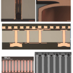
Through Silicon Via (TSV):
Through silicon vias (TSVs) are holes created in a silicon wafer using an etch process. Interconnects are formed by filling TSVs with a conductive material, such as copper as seen in the figure below. The main advantage of TSV interconnects is the shortened path for the signal to travel from one chip to the next, or one layer of circuitry to the next. This allows for reduced power, and the ability to increase interconnect density, thereby increasing functionality and performance. TSVs are not 3D ICs all by themselves. Rather, they are the building blocks that enable 3D ICs. Backside vias are also used in other devices such as image sensors, microelectromechanical systems (MEMS) and compound semiconductors.
_
Compared to traditional 2D architecture, 3D ICs provide several significant advantages:
-1. Footprint
Obviously, stacking multiple dies atop one another produces a chip that takes up less space than if those dies were side by side. If the layers are aggressively thinned, a multi-layer 3D-IC is actually no thicker than a traditional 2D chip. The tiny size of 3D-ICs is extremely valuable in miniaturized devices such as cell phones and IoT applications.
-2. Speed
Dies stacked in a 3D chip are much closer together than chips on a circuit board. The shorter distances allow electronic signals to travel more quickly from one component to another. 3D stacked devices have shown as much as 5x speed improvement over comparable 2D solutions.
-3. Power
Shorter connections automatically require less power, but 3D ICs have another power-saving trick. When an electronic signal travels from one chip to another, it passes through special circuitry that screens out any accidental electrostatic discharge (ESD). These ESD filters consume energy. Signals that travel from one layer to another within a 3D-IC do not require ESD checks. Tests have seen as much as 90% reduction in power consumption.
_
Heterogeneous Integration:
Because the layers in a 3D IC are manufactured separately, they can be built differently. This is more important than it might seem! The process in which a die is built affects the behavior of the components on that die: one process makes better capacitors, another makes faster transistors, etc. Even more interesting, the layers may be built at different process nodes – that is, the electronic components may differ in size. This affects the cost, complexity, and performance of each layer. It is even possible to stack layers that are built of different materials. All of these possibilities mean that a 3D IC can combine the best of each process, node, and substrate without compromising some components to accommodate others. In fact, a multi-die stack can contain combinations that are flatly impossible to achieve on a 2D chip.
_
There are a few major hurdles to overcome for 3D ICs:
First, every die in the stack must be designed for stacking, and that design effort is considerable. If different entities are responsible for the different layers, close collaboration is essential from initial design through final test.
Second, the manufacturing steps must be carefully coordinated. Different layers can be processed by different manufacturers, and they are most likely stacked at yet another facility.
In specific markets such as memories and sensors, the immediate benefits of 3D far outweigh the difficulties. Successes in these initial markets are already establishing precedents for future designs. As the 3D architecture matures, the industry will see a steady increase in ambitious, ground-breaking 3D projects. 3D is clearly the technology of the future! Today, only a select few companies have mastered 3D. They have built the necessary relationships, created the supply chain, acquired the skills and experience, and actually produced working 3D ICs.
_
3D packaging refers to 3D integration schemes that rely on traditional methods of interconnect at the package level such as wire bonding and flip chip to achieve vertical stacks. Examples of 3D packages include package-on-package (PoP) where individual die are packaged, and the packages are stacked and interconnected with wire bonds or flip chip processes; and 3D wafer-level packaging (3D WLP) that uses redistribution layers (RDL) and bumping processes to form interconnects.
2.5D interposer is a configuration where dies are mounted side-by-side on a silicon, glass, or organic interposer using through silicon vias (TSVs) through the interposer. (When glass or organic laminate is used as the interposer substrate, the vias are called through glass vias (TGV) and through substrate via (TSV) respectively.) Communication between the dies takes place via circuitry fabricated on the interposer.
CMOS image sensors (CIS) have TSVs as backside vias to form interconnects, eliminate wire bonds, and allow for reduced form factor and higher-density interconnects. In all types of 3D packaging, chips in the package communicate using off-chip signaling, much as if they were mounted in separate package on a normal circuit board.
______
______
Moore’s Law:
Integrated circuits revolutionized electronics and computing during the 1960s and 1970s. First, engineers were putting dozens of components on a chip in what was called Small-Scale Integration (SSI). Medium-Scale Integration (MSI) soon followed, with hundreds of components in an area the same size. Predictably, around 1970, Large-Scale Integration (LSI) brought thousands of components, Very-Large-Scale Integration (VLSI) gave us tens of thousands, and Ultra Large Scale (ULSI) millions—and all on chips no bigger than they’d been before. In 1965, Gordon Moore of the Intel Company, a leading chip maker, noticed that the number of components on a chip was doubling roughly every one to two years. Moore’s Law, as this is known, has continued to hold ever since. Interviewed by The New York Times 50 years later, in 2015, Moore revealed his astonishment that the law has continued to hold: “The original prediction was to look at 10 years, which I thought was a stretch. This was going from about 60 elements on an integrated circuit to 60,000—a thousandfold extrapolation over 10 years. I thought that was pretty wild. The fact that something similar is going on for 50 years is truly amazing.”
Five decades of Moore’s law:
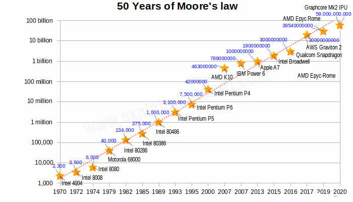
The chart above showing the exponential growth in transistor counts for common microchips from 1970 to the present. The number of transistors packed into microchips has roughly doubled every year or two for the last five decades—in other words, it’s grown exponentially. If you plot the number of transistors (y-axis) against the year of launch (x-axis) for some common microchips from the last few decades (yellow stars), you’ll get an exponential curve; plotting the logarithm instead, you’ll get this straight line. Please note that the vertical (y) axis of this chart is logarithmic and the horizontal (x) axis is only vaguely linear.
Named after Intel cofounder Gordon E. Moore. Moore’s Law postulates that the number of transistors embedded in an integrated circuit doubles every 2 years, while the price remains the same. As of 2019, the most advanced microprocessors contain nearly 40 billion transistors. The number of transistors defines capability (e.g., processing capabilities, speed, and memory). Additionally increased number of microscopic transistors per unit area reduced cost, improved performance, decreased power consumption and occupied less space. Cost is low because millions of transistors are printed as a complete unit by photolithography and not constructed as one transistor at a time. As transistors get smaller, they switch faster and use less energy. Smaller is the transistor lesser is the distance between source & drain, lesser number of electrons/ holes are required to form the conducting channel below gate. Lesser input voltage is required to generate hence less power consumption and it switches faster as lesser distance to be travelled by electrons/ holes. Performance is higher since the components switch quickly, consuming little power.
Moore’s Law has propelled the semiconductor industry forward, because it proved to be lucrative to be first-to-market with a new generation of smaller, denser, more powerful chips. And thanks to scaling, the cost of Logic and Memory chips has been reduced so dramatically that it’s now possible to put a chip in practically anything, opening up a world of possibilities for connected and smart devices in IoT (the internet of things). This expansion of possibilities is what continues to drive the growth of the €412 billion (2019) global semiconductor industry.
Delivering higher performance at lower cost with each chip generation, the relentless pace of Moore’s Law has changed the world we live in. Doubling the number of transistors on a chip has enabled consumer products that were once the stuff of dreams. A single smartphone today has far more computing power than the computers used by NASA for the Apollo 11 moon landing in 1969.
7nm process ICs represent the newest wave of chips in electronic devices and enable better performance per watt than previous generation ICs. Higher density designs pack more components into a smaller space for greater functionality (such as for artificial intelligence and machine learning applications) and can offer increased energy efficiency.
As electronic devices become smaller and more ubiquitous, putting more transistors on a chip is the way we can continue to bring more value, more functionality, lower cost and lower power consumption. From a systems perspective, we continue to put more and more transistors on a chip so we can have more and more complex functions, integrate them to increase performance of our systems and reduce power.
_____
_____
Roadblocks to Moore’s law:
By 2015, Moore forecast that the rate for increasing IC density would reach a point of saturation within the next decade or so—as transistor miniaturization reaches a fundamental barrier at the atomic level. The transistor count for AMD’s 2nd generation EPYC™ server CPU launched in 2019 has reached nearly 40 billion. Some fundamental limits loom less than a decade away. Top-of-the-line microprocessors currently have circuit features that are around 14 nanometers across, smaller than most viruses. But even with super-aggressive efforts, we’ll get to the 2–3-nanometre limit, where features are just 10 atoms across. Is that a device at all? Probably not — if only because at that scale, electron behaviour will be governed by quantum uncertainties that will make transistors hopelessly unreliable. We cannot infinitely diminish the size of the chips. There is a limit at which they stop working correctly. When it comes down to the nanometer size, electrons escape from the channels where they circulate through the so-called “tunnel effect”, a typically quantum phenomenon. Electrons are quantum particles and they have wave-like behavior, hence, there is a possibility that a part of such electrons can pass through the walls between which they are confined. Under these conditions the chip stops working properly. Signals can “bleed” more easily between them. Tiny matter obeys the rules of quantum mechanics, which are quite different from the classical rules that determine the properties of conventional logic gates. And despite vigorous research efforts, there is no obvious successor to today’s silicon technology. As they get smaller, they become much harder to imprint on the chips. And their very scale and proximity can affect electrical properties.
Other challenges:
-1. The latest, greatest, and smallest transistors are also the trickiest and most expensive to design and manufacture with. Improving a microprocessor’s performance meant scaling down the elements of its circuit so that more of them could be packed together on the chip. Scaling, in turn, required major refinements in photolithography, the basic technology for etching those microscopic elements onto a silicon surface. But the boom times were such that this hardly mattered: a self-reinforcing cycle set in. Chips were so versatile that manufacturers could make only a few types — processors and memory, mostly — and sell them in huge quantities. That gave them enough cash to cover the cost of upgrading their fabrication facilities, or ‘fabs’, and still drop the prices, thereby fuelling demand even further. Soon, however, it became clear that this market-driven cycle could not sustain the relentless cadence of Moore’s law by itself. The chip-making process was getting too complex, often involving hundreds of stages, which meant that taking the next step down in scale required a network of materials-suppliers and apparatus-makers to deliver the right upgrades at the right time. Every time the scale is halved, manufacturers need a whole new generation of ever more precise photolithography machines. Building a new fab line today requires an investment typically measured in many billions of dollars — something only a handful of companies can afford. And the fragmentation of the market triggered by mobile devices is making it harder to recoup that money. As soon as the cost per transistor at the next node exceeds the existing cost, the scaling stops. Many observers think that the industry is perilously close to that point already. We run out of money before we run out of physics.
-2. The doubling of transistors per unit area of chip has already started to falter, thanks to the heat that is unavoidably generated when more and more silicon circuitry is jammed into the same small area. Nothing is 100% efficient. Wires have resistance. Transistors have little resistance. Every flow of electrical energy necessarily has some inefficiency. Energy can’t be destroyed, so where does this lost electrical energy go? Heat. A transistor (FET, in modern ICs) never switches instantly from full OFF to full ON. There is a period while it’s turning on or off where the FET acts like a resistor (even when fully ON it still has a resistance). As you know, passing a current through a resistor generates heat. The more the transistors switch the more time they spend in that resistive state, so the more heat they generate. So the amount of heat generated can be directly proportional to the number of transistors – but it is also dependent on which transistors are doing what and when, and that depends on what the chip is being instructed to do. The faster your processor runs, the more power it requires and the more heat it generates. That was a fundamental problem. Heat is hard to get rid of, and no one wants to buy a mobile phone that burns their hand. So manufacturers seized on the only solutions they had.
First, they stopped trying to increase ‘clock rates’ — how fast microprocessors execute instructions. This effectively put a speed limit on the chip’s electrons and limited their ability to generate heat. The maximum clock rate hasn’t budged since 2004.
Second, to keep the chips moving along the Moore’s law performance curve despite the speed limit, they redesigned the internal circuitry so that each chip contained not one processor, or ‘core’, but two, four or more. This is the introduction of partitioned multi-die design (Chiplet), which allows a semiconductor company to interconnect many smaller and lower core dies together to make a CPU with a greater number of cores. You can have the same output with four cores going at 250 megahertz as one going at 1 gigahertz. However, in practice, exploiting 4 processors means that a problem has to be broken down into 4 pieces — which for many algorithms is difficult to impossible. A Chiplet design may also increase the yield of acceptable products in manufacturing. AMD estimates that the multi-die approach reduces manufacturing costs by about forty percent.
_
Advanced packaging:
As it becomes more difficult to manufacture ever smaller transistors, companies are using multi-chip modules, three-dimensional integrated circuits, package on package, High Bandwidth Memory and through-silicon vias (TSVs) with die stacking to increase performance and reduce size, without having to reduce the size of the transistors. Such techniques are collectively known as advanced packaging. Advanced packaging is mainly divided into 2.5D and 3D packaging. 2.5D describes approaches such as multi-chip modules while 3D describes approaches where dies are stacked in one way or another, such as package on package and high bandwidth memory. All approaches involve 2 or more dies in a single package. Alternatively, approaches such as 3D NAND stack multiple layers on a single die.
______
______
Types of Chips produced by Semiconductor Companies:
The types of chips produced by semiconductor companies can be categorized in many ways. Usually, chips are categorized in terms of their functionality. However, they are sometimes divided into types according to the integrated circuits (ICs) used. When looked at according to functionality, the four main categories of semiconductors are memory chips, microprocessors, standard chips, and complex systems-on-a-chip (SoCs). When organized by types of integrated circuitry, the three types of chips are digital, analog, and mixed.
_
Chip types based on functionality:
Memory Chips:
From the perspective of functionality, semiconductor memory chips store data and programs on computers and data storage devices. Random-access memory (RAM) chips provide temporary workspaces, whereas flash memory chips hold information permanently unless erased. Read-only memory (ROM) and programmable read-only memory (PROM) chips cannot be modified. In contrast, erasable programmable read-only memory (EPROM) and electrically erasable read-only memory (EEPROM) chips can be changed.
Microprocessors:
Microprocessors contain one or more central processing units (CPUs). Computer servers, personal computers (PCs), tablets, and smartphones may each have multiple CPUs. The 32- and 64-bit microprocessors in PCs and servers today are based on x86, POWER, and SPARC chip architectures, first developed decades ago. On the other hand, mobile devices like smartphones typically use an ARM chip architecture. Less powerful 8-, 16- and 24-bit microprocessors (called microcontrollers) turn up in products such as toys and vehicles.
Graphic Processing Units (GPUs):
Technically a type of microprocessor, Graphics Processing Unit (GPU) is capable of rendering graphics for display on an electronic device. A GPU is a specialized processor whose job is to rapidly manipulate memory and accelerate the computer for a number of specific tasks that require a high degree of parallelism. The GPU was introduced to the wider market in 1999 and is best known for its use in providing the smooth graphics that consumers expect in modern videos and games. Before the arrival of GPUs in the late 1990s, graphic rendering was handled by the Central Processing Unit (CPU). When used in conjunction with a CPU, a GPU can increase computer performance by taking on some computationally-intensive functions, such as rendering, from the CPU. This accelerates how quickly applications can process since the GPU can perform many calculations simultaneously. This shift also allowed for the development of more advanced and resource-intensive software and activities such as cryptocurrency mining.
Commodity ICs:
Commodity integrated circuits (CICs), are simple chips used for performing repetitive processing routines. Produced in large batches, these chips are generally used in single-purpose appliances such as barcode scanners. Characterized by razor-thin margins, the commodity IC market is dominated by large Asian semiconductor makers. If an IC is made for a specific purpose, it is called an ASIC, or application-specific integrated chip. For example, bitcoin mining today is accomplished with ASICs that only do that one function: mining. Field-programmable gate arrays (FPGA chips) are another type of commoditized IC that can be customized to a manufacturer’s specifications.
The SoC (system on a chip) is among the newest type of chip and the most welcoming to new manufacturers. In the SoC, all of the electronic components needed for an entire system are built into a single chip. The capabilities of a SoC are more extensive than those of a microcontroller chip, which generally combines the CPU with RAM, ROM, and input/output (I/O). In a smartphone, the SoC may also integrate graphics, camera, and audio and video processing. Adding a management chip and a radio chip results in a three-chip solution.
Taking the other approach to categorizing chips, most computer processors currently use digital circuits. These circuits usually combine transistors and logic gates. Sometimes, microcontrollers are added. Digital circuits use digital, discrete signals that are generally based on a binary scheme. Two different voltages are assigned, each representing a different logical value.
_
Chip types based on integrated circuitry:
There are two primary types of IC: digital ICs and analog ICs.
Each kind of microchip performs a different task, and is identified by a code number. Some microchips work with analog signals (a microchip with code 741 is an analog amplifier). Others work with digital signals to act as LOGIC GATES, or to get digital sound from a CD.
Analog Integrated Circuits:
In this type, the input and output are continual, varying signals operating over a continuous range. The output signal level is a linear function of the input level. The voltages are directly proportional to each other. That is why this type is also called “linear ICs.” Linear ICs are used most often for frequency amplification. Well-known examples of this type of IC are voltage regulators, timers, comparators, and operational amplifiers. Op-amps are the most common and include resistors, diodes, and transistors. Linear ICs are crucial in audio amplifiers, sweep generators, audio filters, and oscillators.
Digital Integrated Circuits:
A digital IC has a finite number of discrete input and output states. Digital circuits are also called “non-linear ICs” because they work on discontinuous, binary signals. The input and output voltages of non-linear ICs have two possible values. These values, the “high” or “low” voltage, will result in different gated outputs. These circuits work as logical operators to calculate Boolean functions. This type of IC is used for digital logic gates such as the AND gate, OR gate, NAND gate, XOR gate, flip flips, and counters. These ICs are used to control the flow of processes in systems. They are crucial for programmable devices, memory chips, and logic boards such as microprocessors and microcontrollers.
Analog versus digital circuits:
Analog, or linear, circuits typically use only a few components and are thus some of the simplest types of ICs. Generally, analog circuits are connected to devices that collect signals from the environment or send signals back to the environment. For example, a microphone converts fluctuating vocal sounds into an electrical signal of varying voltage. An analog circuit then modifies the signal in some useful way—such as amplifying it or filtering it of undesirable noise. Such a signal might then be fed back to a loudspeaker, which would reproduce the tones originally picked up by the microphone. Another typical use for an analog circuit is to control some device in response to continual changes in the environment. For example, a temperature sensor sends a varying signal to a thermostat, which can be programmed to turn an air conditioner, heater, or oven on and off once the signal has reached a certain value.
A digital circuit, on the other hand, is designed to accept only voltages of specific given values. A circuit that uses only two states is known as a binary circuit. Circuit design with binary quantities, “on” and “off” representing 1 and 0 (i.e., true and false), uses the logic of Boolean algebra. (Arithmetic is also performed in the binary number system employing Boolean algebra.) These basic elements are combined in the design of ICs for digital computers and associated devices to perform the desired functions.
Mixed-Signal Integrated Circuits:
These hybrid designs are engineered by combining elements of analog and digital ICs. In real-life applications, mixed ICs are everywhere. These ICs make it possible to have chips that act as A/D (analog-to-digital) converters, D/A (digital-to-analog) converters, and clock timing circuits. Modern computing is based upon these circuits.
_
Chip types based upon the techniques used while manufacturing and assembling them:
Monolithic ICs:
Monolithic integrated circuits are fabricated entirely upon a single chip. It has the full circuit constructed on a single piece of semiconductor, enclosed in a chassis, and then given connecting leads. It is small in size compared to hybrids. All the components are formed together by a method such as diffusion or ion implantation. These chips are typically more expensive, operated at high speeds, and provide little flexibility in circuit design.
Hybrid/Multichip ICs:
Hybrid integrated circuits are made by interconnecting several individual chips. The chip is often a ceramic substrate with one or more silicon chips attached. It may also use other semiconductors, such as gallium arsenide chips. These chips are larger compared to monolithic ICs. The elements of the hybrid circuit are typically connected by TEM mode transmission lines. These chips tend to be less expensive, slower due to their connections, and result in greater flexibility in circuit design.
Rugged ICs:
Rugged ICs are created by using silicon carbide as this semiconducting material can withstand high voltage and possess high thermal conductivity. Rugged ICs are far superior than usual ICs, in terms of built quality and design and thus they provide better performance to electrical devices. These advanced ICs improve efficiency of the analog and digital circuits and are extensively used in different sectors such as electronics, power generation, automobile, and aerospace.
Thin and Thick Film ICs:
These devices are larger than monolithic ICs but smaller than discrete circuits. These ICs can be used when power requirement is comparatively higher. With a thin- or thick-film IC, the passive components like resistors and capacitors are integrated, but the transistors and diodes are connected as discrete components to form a complete circuit. Therefore, commercially available thin- and thick-film circuits are combination of integrated and discrete components. The essential difference between the thin- and thick-film ICs is not their relative thickness but the method of deposition of film. Both have similar appearance, properties and general characteristics.
Thin-film ICs:
Thin-film ICs are fabricated by depositing films of conducting material on the surface of a glass or ceramic base. By controlling the width and thickness of the films and by using different materials selected for their resistivity, resistors and conductors are fabricated. Capacitors are produced by sandwiching a film of insulting oxide between two conducting films. Inductors are made by depositing a spiral formation of film. Transistors and diodes can be produced by thin-film technology; but usually tiny discrete components are connected into the circuit.
One method used for producing thin films is vacuum evaporation in which vapourized material is deposited on a substrate contained in a vacuum. In other method, called cathode sputtering, atoms from a cathode made of the desired film material are deposited on a substrate located between a cathode and an anode.
Thick-film ICs:
Thick-film ICs are sometimes referred to as printed thin-film circuits. In their manufacturing process silk-screen printing techniques are used to create the desired circuits pattern on a ceramic substrate. The screens are actually made of fine stainless steel wire mesh, and the inks are pastes having conductive, resistive, or dielectric properties. After printing, the circuits are high temperature-fired in a furnace to fuse the films to the substrate. Thick-film passive components are fabricated in the same way as those in thin-film circuits. As with thin-film circuits, active components are added as separate devices.
ICs produced by thin- or thick-film techniques have the advantages of forming passive components with wider range and better tolerances, better isolation between their components, greater flexibility in circuit design and of providing better high-frequency performance than monolithic ICs. However, such ICs suffer from the drawbacks of larger physical size, comparatively higher cost and incapability of fabrication of active components.
_
Chip types based on Instruction Set Architecture (ISA): CISC and RISC:
The architecture of the Central Processing Unit (CPU) operates the capacity to function from “Instruction Set Architecture” to where it was designed. The architectural design of the CPU is Reduced instruction set computing (RISC) and Complex instruction set computing (CISC). CISC has the capacity to perform multi-step operations or addressing modes within one instruction set. It is the CPU design where one instruction works several low-level acts. For instance, memory storage, loading from memory, and an arithmetic operation.
Reduced instruction set computing is a Central Processing Unit design strategy based on the vision that a basic instruction set gives great performance when combined with a microprocessor architecture. This architecture has the capacity to perform the instructions by using some microprocessor cycles per instruction.
Intel processors (commonly referred to as X86 in correlation with Windows 32-bit programs) use Complex Instruction Set Computing (CISC), while ARM uses Reduced Instruction Set Computing (RISC). While both perform commands rather quickly in 2021, thanks to multiple cores, CISC uses a slightly more complex instruction set, which requires several cycles to perform tasks. The main idea is complex hardware and simple software. In this case, it means more basic assembly language functionality.
ARM processors use only one cycle to execute a command, reducing functions. This feature makes ARM processors ideal for power consumption-conscious devices, i.e., mobile and embedded devices. The core concept behind RISC is simple hardware and complex software. Greater functionality at lower-level programming languages. Assembly, in this case, can be a real game-changer when it comes to reducing power consumption.
Making this up for the sake of an example, a CISC chip might have instructions for painting a two-story house, painting a one-story house, painting a toolshed, and painting a playhouse. A RISC chip would just have an instruction for painting a wall. In order to paint any of those structures, the software has to issue the “paint a wall” instruction several times for each kind of wall.
The problem with CISC chips that they end up being very complex with a lot of instructions that are not often used and might get overlooked. The chip runs hot and slow since it has so much internal “machinery.” Also, the complexity makes it hard to scale down the architecture, say from 12nm to 10nm. Scaling down the architecture makes the chip faster, but it runs hotter, because the CISC chip has so much to do.
RISC chips are much simpler and run cooler, but software needs to give them more instructions to do the same job. It ends up being simpler, faster, and more efficient because the chip is always being optimally used. It is easier to scale down the architecture to speed up a RISC chip. Since it is simpler, other features can be added to the chip.
______
______
Chip’s Cultural Connections:
Since their appearance, microchips have transformed much of human society. They are now found in computers, guided missiles, “smart” bombs, satellites for communications or scientific exploration, hand-held communications devices, televisions, aircraft, spacecraft, and motor vehicles. Without microchips, such familiar devices as the personal computer, cell phone, personal digital assistant, calculator, Global Positioning System, and video game would not exist. As chip complexity increases and cost decreases thanks to improvements in manufacturing techniques, new applications for chips are constantly being found. It would, then, be difficult to name a department of human activity that has not been affected by the microchip.
However, efforts to replace the printed paper book with electronic texts (e-books) downloaded to computers or other chip-based viewing devices have repeatedly failed; also, lot of people still live in poverty and do not have access to sufficient food, clean water, or medical care, much less to a computer; and despite early predictions of a “paperless office,” per capita paper consumption has risen, not fallen, since the advent of the microchip. Additionally, studies have found that persons who spend more time each day surfing the Web are more likely to suffer depression, probably as a result of decreased time spent with family and friends.
The microchip has produced few entirely new pastimes or economic activities. It has tended to modify existing patterns of human activity—personal, political, military, medical and economic—but not to transform them out of all recognition or to eliminate them. Quantum computing and other novel techniques are being intensively researched by governments and industries, but all still had to cross major technological hurdles before they could rival silicon’s cheapness, speed, and device density.
_______
_______
Advantages and disadvantages of ICs:
ICs have two main advantages over discrete circuits: cost and performance. The cost is low because the chips, with all their components, are printed as a unit by photolithography rather than being constructed one transistor at a time. Furthermore, packaged ICs use much less material than discrete circuits. Performance is high because the IC’s components switch quickly and consume comparatively little power because of their small size and proximity.
Some advantages of semiconductor ICs which makes them highly useful everywhere:
- They are highly portable due to the smaller size
- They require less input power
- Semiconductor devices are shockproof
- They have a longer lifespan
- They are noise-free while operating
The main disadvantage of ICs is the high cost of designing them and fabricating the required photomasks. They are difficult to design and manufacture, and need very expensive machinery to fabricate. This high initial cost means ICs are only commercially viable when high production volumes are anticipated. The robotic processes must operate on a microscopic level. Super-clean, dust-free, precise climate control and clean suits for the workers are a must. Even in perfect conditions, there are a lot of failed chips in the wafers that are produced. Also, ICs are susceptible to electrostatic discharge (ESD), electromagnetic pulse (EMP) and physical damage; and must be packaged well and handled carefully.
______
______
Section-4
History of semiconductor:
Some of the properties of semiconductor materials were observed throughout the mid-19th and first decades of the 20th century. The first practical application of semiconductors in electronics was the 1904 development of the cat’s-whisker detector, a primitive semiconductor diode used in early radio receivers. Developments in quantum physics led in turn to the invention of the transistor in 1947, the integrated circuit in 1958, and the MOSFET (metal–oxide–semiconductor field-effect transistor) in 1959.
The birth history of semiconductors can be traced back to the invention of the rectifier (AC-DC converter) in 1874. Decades later, Bardeen and Brattain at Bell Laboratories in the US invented the point-contact transistor in 1947, and Shockley invented the junction transistor in 1948. This heralded the arrival of the transistor era. In 1946, the University of Pennsylvania in the US built a computer using the vacuum tubes. The computer was so large that its vacuum tubes occupied the entire building, and it consumed a huge amount of electricity and produced a lot of heat. Later, the innovative transistor calculator (computer) was developed, and since then computers have grown by leaps and bounds. In 1956, the Nobel Prize in Physics was awarded jointly to Shockley, Bardeen and Brattain for their contribution to semiconductor research and the development of the transistor.
The semiconductor industry grew rapidly following the invention of the transistor. In 1957, it already exceeded the scale of 100 million dollars. In 1959, the bipolar integrated circuit (ICs) was invented by Kilby of Texas Instruments and Noyce of Fairchild Semiconductor in the US. This invention had a major impact on the history of semiconductors, and it marked the dawn of the IC era. Being small in size and light in weight, the IC was widely used in a variety of electric appliances.
In 1967, Texas Instruments developed the electronic desktop calculator (the calculator) using IC. In Japan, electronic equipment manufacturers released calculators one after another, and fierce “calculator wars” continued until the end of the 1970s. IC integration advanced even further, and the large-scale integrated circuit (LSI) was developed. The technologies continue to advance. The VLSI (from 20 thousand to 1 million electronic components per chip) was developed in the 1980s, and the ULSI (more than 1 million electronic components per chip) was developed in the 1990s. In the 2000s, the system LSI (a multifunction LSI with multiple functions integrated in a single chip) was put into full-scale production. As IC progresses toward high performance and multiple functions, its field of application is expanding broadly. Semiconductors are now used in every corner of our society and support everyday life.
_
Brief history of semiconductor is depicted in the figure below:
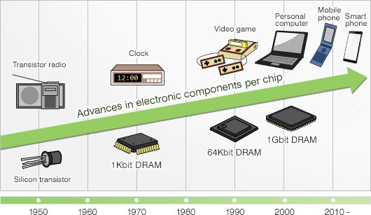
_
Invention of IC:
The electronics revolution was built on developments in three distinct fields: human-computer interface, which connected people to their machines; networking, which connected the machines together; and, most importantly, microchips – the machines themselves. The U.S. government unquestionably played the decisive role in the development of the first two fields. The history of the microchip, however, which powers everything from computers to cell phones to CD players, contained many contributions from both government and industry, in America and abroad. In fact, the microchip arguably began in the laboratory of the newly-formed Texas Instruments with the creation of the first integrated circuit.
In 1958 and 1959, two people had the idea for an integrated circuit at almost exactly the same time. Transistors had become an everyday thing used in household devices such as radios. They affected everything from radios to phones and at the time manufacturers needed a smaller replacement for vacuum tubes. Transistors were smaller than vacuum tubes, but for some of the newest electronics, for example missile guidance, they were not small enough. The air competition from 1950 to 1960 was fierce. In order to do more in the limited space of the spacecraft, the United States requires that the equipment be small, so that more electronic equipment can be installed in a small space, thereby developing chips. Up to this point, each component in an electronic circuit had to be individually connected by wires. In September 1958. Jack Kilby of Texas Instruments demonstrated the first integrated circuit, which was fabricated in germanium. At about the same time, Robert Noyce of Fairchild Semiconductor introduced the integrated circuit in silicon using a planar technology. The first circuit used bipolar transistors. Practical MOS transistors were then developed in the mid-’60s. The MOS technologies, especially CMOS, have become major focus for IC design and development. Many manufacturers quickly took advantage of the small size of the chip and the low current consumption to further produce microcomputers and microcomputers.
One day in July, Jack Kilby was working at Texas Instruments when it occurred to him that all parts of a circuit, not just the transistor, could be made out of silicon. At the time, nobody was putting capacitors and resistors into ICs. This would change the future and make it easier to produce and sell integrated circuits. Kilby’s boss liked the idea, and told him to get to work. Kilby came upon the idea he called the monolithic principle: trying to build all the different parts of an electronic circuit on a silicon chip. On September 12, 1958, he hand-built the world’s first, crude integrated circuit using a chip of germanium (a semiconducting element similar to silicon) and Texas Instruments applied for a patent on the idea the following year.
Meanwhile, at another company called Fairchild Semiconductor (formed by a small group of associates who had originally worked for the transistor pioneer William Shockley) the equally brilliant Robert Noyce was experimenting with miniature circuits of his own. In 1959, he used a series of photographic and chemical techniques known as the planar process (which had just been developed by a colleague, Jean Hoerni) to produce the first, practical, integrated circuit, a method that Fairchild then tried to patent.
Integrated circuit patent diagrams from 1959 by Jack Kilby of Texas Instruments and Robert Noyce of Fairchild Semiconductor, compared side by side. Two great electrical engineers, Jack Kilby and Robert Noyce, came up with the same idea at almost exactly the same time in 1959. Although Kilby filed his patent first, Noyce’s patent was granted earlier. Today, both men are acknowledged as having independently conceived of the idea. Kilby and Noyce are now rightly regarded as joint-inventors of arguably the most important and far-reaching technology developed in the 20th century. Both men were inducted into the National Inventors Hall of Fame (Kilby in 1982, Noyce the following year) and Kilby’s breakthrough was also recognized with the award of a half-share in the Nobel Prize in Physics in 2000 (as Kilby very generously noted in his acceptance speech, Noyce would surely have shared in the prize too had he not died of a heart attack a decade earlier).
_
MOSFET (MOS transistor):
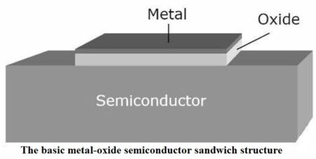
In the late 1950s, Mohamed Atalla utilized his surface passivation and thermal oxidation methods to develop the metal–oxide–semiconductor (MOS) process, which he proposed could be used to build the first working silicon field-effect transistor. This led to the invention of the MOSFET (MOS field-effect transistor) by Mohamed Atalla and Dawon Kahng in 1959. It was the first truly compact transistor that could be miniaturised and mass-produced for a wide range of uses. With its scalability, and much lower power consumption and higher density than bipolar junction transistors, the MOSFET became the most common type of transistor in computers, electronics, and communications technology such as smartphones. The US Patent and Trademark Office calls the MOSFET a “ground-breaking invention that transformed life and culture around the world”. The metal–oxide–semiconductor field-effect transistor (MOSFET), also known as the metal–oxide–silicon transistor (MOS transistor, or MOS), is a type of insulated-gate field-effect transistor that is fabricated by the controlled oxidation of a semiconductor, typically silicon.
The CMOS (complementary MOS) process was developed by Chih-Tang Sah and Frank Wanlass at Fairchild Semiconductor in 1963. The first report of a floating-gate MOSFET was made by Dawon Kahng and Simon Sze in 1967. FinFET (fin field-effect transistor), a type of 3D multi-gate MOSFET, was developed by Digh Hisamoto and his team of researchers at Hitachi Central Research Laboratory in 1989.
__
A major reason for the success of silicon ICs is the fact that an excellent native oxide, SO2, can be formed on the surface of silicon. This oxide is used as a gate insulator in the MOSFET and is also used as an insulator, known as the field oxide, between devices. Metal interconnect lines that connect various devices can be placed on top of the field oxide. Most other semiconductors do not form native oxides that are of sufficient quality to be used in device fabrication. Silicon will oxidize at room temperature in air forming a thin native oxide of approximately 25 A thick. However, most oxidations are done at elevated temperatures during fabrication of ICs since the basic process requires that oxygen diffuse through the existing oxide to the silicon surface where a reaction can occur.
______
______
Section-5
Semiconductors:
The electrical conductivity of a semiconductor is between that of a good conductor (like copper) and that of an insulator (like rubber). Hence, the name semiconductor. Diodes, transistors, and many photovoltaic cells contain semiconductive material. A Semiconductor can be defined as a material that has the characteristics and ability to conduct a small amount of electrical current in a controlled manner. A semiconductor is a material that has certain unique properties in the way it reacts to electrical current. It is a material that has much lower resistance to the flow of electrical current in one direction than in another. The electrical conductivity of a semiconductor can be controlled over a wide range, either permanently or dynamically. A semiconductor is also a material whose electrical conductivity can be altered (called doping) through variations in temperature, applied fields, or adding impurities. At low temperatures, semiconductors allow little or no conductivity and act as insulators. At room temperature or when exposed to light, voltage, or heat, however, they can conduct electricity. It is this quasi state between conductors and insulators that makes semiconductors so important to electronic devices, as they control how, when, and where electricity flows. Silicon is the most widely used semiconductor material. Few other materials used in making semiconductor are germanium, gallium arsenide, and silicon carbide. There are many other semiconductors. Even certain plastics can be semiconducting, allowing for plastic light-emitting diodes (LEDs) that are flexible and can be molded to any desired shape.
_
A semiconductor material has an electrical conductivity value falling between that of a conductor, such as metallic copper, and an insulator, such as glass. Its resistivity falls as its temperature rises; metals behave in the opposite way. Its conducting properties may be altered in useful ways by introducing impurities (“doping”) into the crystal structure. When two differently doped regions exist in the same crystal, a semiconductor junction is created. The behavior of charge carriers, which include electrons, ions, and electron holes, at these junctions is the basis of diodes, transistors, and most modern electronics. Some examples of semiconductors are silicon, germanium, gallium arsenide, and elements near the so-called “metalloid staircase” on the periodic table. After silicon, gallium arsenide is the second-most common semiconductor and is used in laser diodes, solar cells, microwave-frequency integrated circuits, and others. Silicon is a critical element for fabricating most electronic circuits. Semiconductor devices can display a range of useful properties, such as passing current more easily in one direction than the other, showing variable resistance, and having sensitivity to light or heat. Because the electrical properties of a semiconductor material can be modified by doping and by the application of electrical fields or light, devices made from semiconductors can be used for amplification, switching, and energy conversion.
_
The conductivity of silicon is increased by adding a small amount (of the order of 1 in 10^8) of pentavalent (antimony, phosphorus, or arsenic) or trivalent (boron, gallium, indium) atoms. This process is known as doping, and the resulting semiconductors are known as doped or extrinsic semiconductors. Apart from doping, the conductivity of a semiconductor can be improved by increasing its temperature. This is contrary to the behavior of a metal, in which conductivity decreases with an increase in temperature. The modern understanding of the properties of a semiconductor relies on quantum physics to explain the movement of charge carriers in a crystal lattice. Doping greatly increases the number of charge carriers within the crystal. When a doped semiconductor contains free holes, it is called “p-type”, and when it contains free electrons, it is known as “n-type”. The semiconductor materials used in electronic devices are doped under precise conditions to control the concentration and regions of p- and n-type dopants. A single semiconductor device crystal can have many p- and n-type regions; the p–n junctions between these regions are responsible for the useful electronic behavior. Using a hot-point probe, one can determine quickly whether a semiconductor sample is p- or n-type.
_
Basic semiconductor design:
Any material can be classified as one of three types: conductor, insulator, or semiconductor. A conductor (such as copper or salt water) can easily conduct electricity because it has an abundance of free electrons. An insulator (such as ceramic or dry air) conducts electricity very poorly because it has few or no free electrons. A semiconductor (such as silicon or gallium arsenide) is somewhere between a conductor and an insulator. It is capable of conducting some electricity, but not much.
_
Semiconductors possess specific electrical properties. A substance that conducts electricity is called a conductor, and a substance that does not conduct electricity is called an insulator. Semiconductors are substances with properties somewhere between them. Electrical properties can be indicated by resistivity. The ease with which electricity flows is related to the magnitude of the substance’s electrical resistance. If the electrical resistance is high, the current hardly flows, and if the electrical resistance is low, the electric current flows easily. When electrical conductivity is expressed by resistivity, semiconductors are distributed in the range of 10-6 to 107 Ωcm, whereas conductors are 10-8 to 10-6 Ωcm and insulators are 107 to 1018 Ωcm.
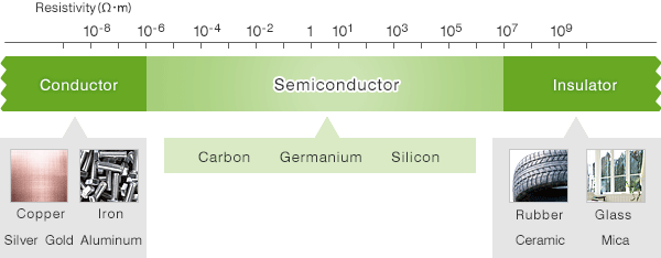
Conductors such as gold, silver and copper have low resistance and conduct electricity easily. Insulators such as rubber, glass and ceramics have high resistance and are difficult for electricity to pass through. Semiconductors have properties somewhere between these two. Their resistivity might change according to the temperature for example. At a low temperature, almost no electricity passes through them. But when the temperature rises, electricity passes through them easily. Semiconductors containing almost no impurities conduct almost no electricity. But when some elements are added to the semiconductors, electricity passes through them easily. Silicon (Si) and germanium (Ge) are well-known semiconductor materials. When they are pure crystals, these substances are close to insulators (intrinsic semiconductors), but doping a small amount of dopant causes the electrical resistance to drop greatly, turning them into conductors. Semiconductors comprising a single element are called elemental semiconductors, including the famous semiconductor material Silicon. On the other hand, semiconductors made up of two or more compounds are called compound semiconductors, and are used in semiconductor lasers, light-emitting diodes, etc.
______
Band Theory of Semiconductors:
An atom is consisting of a nucleus and electrons orbiting the nucleus. The electrons cannot orbit the nucleus at any distance in the atomic space surrounding the nucleus, but only certain, very specific orbits are allowed, and only exist in specific discrete levels. These energies are called energy levels. Electrons arrange themselves in layers called shells inside an atom. The outermost shell in the atom is known as a valence shell. The electrons in this valence shell are the ones that form bonds with neighboring atoms. Such bonds are called covalent bonds. Most conductors have just one electron in the valence shell. Semiconductors, on the other hand, typically have four electrons in their valence shell. However, if atoms nearby are made of the same valence, electrons may bind with the valence electrons of other atoms. Whenever that happens, atoms organize themselves into crystal structures. We make most semiconductors with silicon crystals. A large number of atoms gather to form a crystal, and interacts in a solid material, then the energy levels became so closely spaced that they form bands. This is the energy band. Metals, semiconductors and insulators are distinguished from each other by their band structures.
The important property of electrons is determined by the rule that is called the Pauli exclusion principle. According to this principle, not more than two electrons with different spins can occupy each energy state. Electrons occupy the lowest energy levels first. In semiconductors and insulators, almost all the states in the lowest energy bands are filled by electrons, whereas the energy states in the higher energy bands are, by and large, empty. The lower energy bands with mostly filled energy states are called the valence bands. The higher energy bands with mostly empty energy states are called conduction bands. The difference between the highest valence band and the lowest conduction band is called the energy band gap or the energy gap. An electron in a valence band needs the energy equal to or higher than the energy gap to experience a transition from the valence to the conduction band.
The valence band is the band of electron orbitals that electrons can jump out of, moving into the conduction band when excited. The valence band is simply the outermost electron orbital of an atom of any specific material that electrons actually occupy. This is closely related to the idea of the valence electron.
Conduction band is the outermost electrons are not tightly held to the nucleus due to which sometimes they leave the outermost orbit at room temperature and become free electrons. These free electrons tend to conduct current in conductors and this is the reason they are known as conduction electrons.
The energy difference between the highest occupied energy state of the valence band and the lowest unoccupied state of the conduction band is called the band gap and is indicative of the electrical conductivity of a material. A large band gap means that a lot of energy is required to excite valence electrons to the conduction band. Conversely, when the valence band and conduction band overlap as they do in metals, electrons can readily jump between the two bands (see figure below) meaning the material is highly conductive.
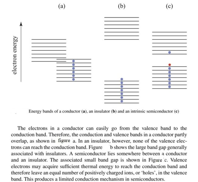
Each silicon atom in the crystal is surrounded by four of its nearest neighbours. Each atom has four electrons in its outer orbit and shares these electrons with its four neighbours. Each shared electron pair constitutes a covalent bond. The force of attraction between the electrons and both nuclei holds the two atoms together. For isolated atoms (e.g., in a gas rather than a crystal), the electrons can have only discrete energy levels. However, when a large number of atoms are brought together to form a crystal, the interaction between the atoms causes the discrete energy levels to spread out into energy bands. When there is no thermal vibration (i.e., at low temperature), the electrons in an insulator or semiconductor crystal will completely fill a number of energy bands, leaving the rest of the energy bands empty. The highest filled band is called the valence band. The next band is the conduction band, which is separated from the valence band by an energy gap (much larger gaps in crystalline insulators than in semiconductors). This energy gap, also called a bandgap, is a region that designates energies that the electrons in the crystal cannot possess. In insulator, the energy gap, Eg, is large so that the valence bands are completely filled and conduction bands are totally devoid of electrons. Typically for insulator, Eg is larger than 5 to 6 eV. The bandgap of diamond, a good crystalline insulator, is 5.5 eV. For semiconductors, energy band gaps vary between 0.1 eV and 3.5 eV. The energy gap of silicon (Si), which is the most important semiconductor material, is approximately 1.12 eV at room temperature. The energy gap of silicon dioxide—the most widely used insulator material in microelectronics—is 9 eV. In a conductor, valence band and conduction band overlap each other and therefore there is no energy/forbidden/band gap in a conductor.
_
The difference between conductors, insulators, and semiconductors can be shown by how large their band gap is. Insulators are characterized by a large band gap, so a prohibitively large amount of energy is required to move electrons out of the valence band to form a current. Conductors have an overlap between the conduction and valence bands, so the valence electrons in such conductors are essentially free. Semiconductors, on the other hand, have a small band gap that allows for a meaningful fraction of the valence electrons of the material to move into the conduction band given a certain amount of energy. This property gives them a conductivity between conductors and insulators, which is part of the reason why they are ideal for circuits as they will not cause a short circuit like a conductor. This band gap also allows semiconductors to convert light into electricity in photovoltaic cells and to emit light as LEDs when made into certain types of diodes. Both these processes rely on the energy absorbed or released by electrons moving between the conduction and valence bands.
_
The highest energy level that an electron can occupy at the absolute zero temperature is known as the Fermi Level. The Fermi level lies between the valence band and conduction band because at absolute zero temperature the electrons are all in the lowest energy state. Due to lack of sufficient energy at 0 Kelvin, the Fermi level can be considered as the sea of fermions (or electrons) above which no electrons exist. The Fermi level changes as the solids are warmed and as electrons are added to or withdrawn from the solid. The Fermi level determines the probability of electron occupancy at different energy levels. The closer the Fermi level is to the conduction band energy, the easier it will be for electrons in the valence band to transition into the conduction band.
In metals, the conduction band and the valence band come very closer to each other and may even overlap, with the Fermi energy Ef somewhere inside. This means that the metal always has electrons that can move freely and so can always carry current. Such electrons are known as free electrons. These free electrons are responsible for current that flows through a metal.
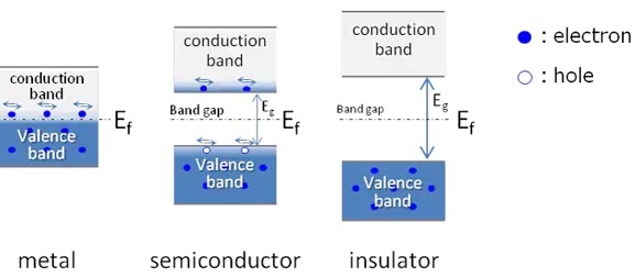
In semiconductors and insulators, the valance band and conduction band are separated by a forbidden energy gap Eg of sufficient width, and the Fermi energy Ef is between the valence and conduction band. To get to the conduction band, the electron has to gain enough energy to jump the band gap. Once this is done, it can conduct.
In semiconductors at room temperature, the band gap is smaller, there is enough thermal energy to allow electrons to jump the gap fairly easily and make the transitions in conduction band, given the semiconductor limited conductivity. At low temperature, no electron possesses sufficient energy to occupy the conduction band and thus no movement of charge is possible. At absolute zero, semiconductors are perfect insulators, The density of electrons in conduction band at room temperature is not as high as in metals, thus cannot conduct current as good as metal. The electrical conductivity of semiconductor is not as high as metal but also not as poor as electrical insulator. That is why, this type of material is called semiconductor – means half conductor.
The band gap for insulators is large so very few electrons can jump the gap. Therefore, current does not flow easily in insulators. The difference between insulators and semiconductors is the size of the band gap energy. In insulator where forbidden gap is very large and as a result the energy required by the electron to cross over to the conduction band is practically large enough. Insulators do not conduct electricity easily. That means the electrical conductivity of insulator is very poor.
_
Semiconductors are defined by their unique electric conductive behavior, somewhere between that of a conductor and an insulator. The differences between these materials can be understood in terms of the quantum states for electrons, each of which may contain zero or one electron (by the Pauli exclusion principle). These states are associated with the electronic band structure of the material. Electrical conductivity arises due to the presence of electrons in states that are delocalized (extending through the material), however in order to transport electrons a state must be partially filled, containing an electron only part of the time. If the state is always occupied with an electron, then it is inert, blocking the passage of other electrons via that state. The energies of these quantum states are critical since a state is partially filled only if its energy is near the Fermi level.
High conductivity in material comes from it having many partially filled states and much state delocalization. Metals are good electrical conductors and have many partially filled states with energies near their Fermi level. Insulators, by contrast, have few partially filled states, their Fermi levels sit within band gaps with few energy states to occupy. Importantly, an insulator can be made to conduct by increasing its temperature: heating provides energy to promote some electrons across the bandgap, inducing partially filled states in both the band of states beneath the band gap (valence band) and the band of states above the bandgap (conduction band). An (intrinsic) semiconductor has a bandgap that is smaller than that of an insulator and at room temperature, significant numbers of electrons can be excited to cross the band gap.
A pure semiconductor, however, is not very useful, as it is neither a very good insulator nor a very good conductor. However, one important feature of semiconductors (and some insulators, known as semi-insulators) is that their conductivity can be increased and controlled by doping with impurities and gating with electric fields. Doping and gating move either the conduction or valence band much closer to the Fermi level and greatly increase the number of partially filled states.
Some wider-bandgap semiconductor materials are sometimes referred to as semi-insulators. When undoped, these have electrical conductivity nearer to that of electrical insulators, however they can be doped (making them as useful as semiconductors). Semi-insulators find niche applications in micro-electronics, such as substrates for HEMT. An example of a common semi-insulator is gallium arsenide. Some materials, such as titanium dioxide, can even be used as insulating materials for some applications, while being treated as wide-gap semiconductors for other applications.
_
Holes and Electrons in Semiconductors:
Holes and electrons are the types of charge carriers accountable for the flow of current in semiconductors. The elevation of electrons from their inner shells to higher shells results in the creation of holes in semiconductors. When the valence electron moves from valence band to the conduction band a vacancy is created in the valence band where electron left. Such vacancy is called hole (electron hole).
The bond model of electrons in silicon of valency 4 is shown below. Here, when one of the free electrons (blue dots) leaves the lattice position, it creates a hole (grey dots). This hole thus created takes the opposite charge of the electron and can be imagined as positive charge carriers moving in the lattice.
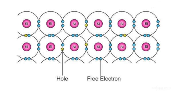
Holes are the positively charged electric charge carrier whereas electrons are the negatively charged particles. Both electrons and holes are equal in magnitude but opposite in polarity. In a semiconductor, the mobility of electrons is higher than that of the holes. It is mainly because of their different band structures and scattering mechanisms. Electrons travel in the conduction band whereas holes travel in the valence band. When an electric field is applied, holes cannot move as freely as electrons due to their restricted movement. Since the holes experience stronger atomic force by the nucleus than electrons, holes have lower mobility. As the electrons move one way, from negative to positive, the holes move the other way, from positive to negative. You can think about current as the flow of electrons, which go from negative to positive, or as the flow of holes, which go the other way.
_
At low temperatures the electrons in a semiconductor are bound in their respective bands in the crystal; consequently, they are not available for electrical conduction. At higher temperatures thermal vibration may break some of the covalent bonds to yield free electrons that can participate in current conduction. Once an electron moves away from a covalent bond, there is an electron vacancy associated with that bond. This vacancy may be filled by a neighbouring electron, which results in a shift of the vacancy location from one crystal site to another. This vacancy may be regarded as a “hole,” that carries a positive charge and moves in a direction opposite to that of an electron. When an electric field is applied to the semiconductor, both the free electrons (now residing in the conduction band) and the holes (left behind in the valence band) move through the crystal, producing an electric current. The electrical conductivity of a material depends on the number of free electrons and holes (charge carriers) per unit volume and on the rate at which these carriers move under the influence of an electric field. In an intrinsic semiconductor there exists an equal number of free electrons and holes. The electrons and holes, however, have different mobilities; that is, they move with different velocities in an electric field. For example, for doped silicon at room temperature, the electron mobility is 1,500 square centimeters per volt-second (cm2/V·s)—i.e., an electron will move at a velocity of 1,500 centimeters per second under an electric field of one volt per centimeter—while the hole mobility is 500 cm2/V·s. The electron and hole mobilities in a particular semiconductor generally decrease with increasing temperature. Mobility decreases with temperature because more carriers are present and these carriers are more energetic at higher temperatures. Each of these facts results in an increased number of collisions and mobility decreases.
Note: The SI unit of velocity is m/s, and the SI unit of electric field is V/m. Therefore the SI unit of mobility is (m/s)/(V/m) = m2/(V.s). However, mobility is much more commonly expressed in cm2/(V⋅s) = 10−4 m2/(V⋅s).
_
Charge carriers as gas:
The partial filling of the states at the bottom of the conduction band can be understood as adding electrons to that band. The electrons do not stay indefinitely (due to the natural thermal recombination) but they can move around for some time. The actual concentration of electrons is typically very dilute, and so (unlike in metals) it is possible to think of the electrons in the conduction band of a semiconductor as a sort of classical ideal gas, where the electrons fly around freely without being subject to the Pauli exclusion principle. In most semiconductors, the conduction bands have a parabolic dispersion relation, and so these electrons respond to forces (electric field, magnetic field, etc.) much as they would in a vacuum, though with a different effective mass. Because the electrons behave like an ideal gas, one may also think about conduction in very simplistic terms such as the Drude model, and introduce concepts such as electron mobility.
For partial filling at the top of the valence band, it is helpful to introduce the concept of an electron hole. Although the electrons in the valence band are always moving around, a completely full valence band is inert, not conducting any current. If an electron is taken out of the valence band, then the trajectory that the electron would normally have taken is now missing its charge. For the purposes of electric current, this combination of the full valence band, minus the electron, can be converted into a picture of a completely empty band containing a positively charged particle that moves in the same way as the electron. Combined with the negative effective mass of the electrons at the top of the valence band, we arrive at a picture of a positively charged particle that responds to electric and magnetic fields just as a normal positively charged particle would do in a vacuum, again with some positive effective mass. This particle is called a hole, and the collection of holes in the valence band can again be understood in simple classical terms (as with the electrons in the conduction band).
_
Carrier generation and recombination:
When ionizing radiation strikes a semiconductor, it may excite an electron out of its energy level and consequently leave a hole. This process is known as electron-hole pair generation. Electron-hole pairs are constantly generated from thermal energy as well, in the absence of any external energy source. Electron-hole pairs are also apt to recombine. Conservation of energy demands that these recombination events, in which an electron loses an amount of energy larger than the band gap, be accompanied by the emission of thermal energy (in the form of phonons) or radiation (in the form of photons). In some states, the generation and recombination of electron-hole pairs are in equipoise. The number of electron-hole pairs in the steady state at a given temperature is determined by quantum statistical mechanics. The precise quantum mechanical mechanisms of generation and recombination are governed by the conservation of energy and conservation of momentum. As the probability that electrons and holes meet together is proportional to the product of their numbers, the product is in the steady-state nearly constant at a given temperature, providing that there is no significant electric field (which might “flush” carriers of both types, or move them from neighbor regions containing more of them to meet together) or externally driven pair generation.
_______
Intrinsic and extrinsic semiconductor:
Semiconductors can be classified as:
- Intrinsic Semiconductor
- Extrinsic Semiconductor
The primary difference between intrinsic and extrinsic semiconductors is their form. For example, intrinsic semiconductors are pure in form and composed of only one kind of material. They do not have any form of impurity added to them.
Metals conduct electricity because their free electrons can move freely between atoms, as electricity requires a flow of electrons from one atom to another. Semiconductors like pure silicon have few free electrons and act more like insulators. These are intrinsic semiconductors. Silicon behavior can be nudged toward conductivity through a process called doping. Doping mixes tiny impurities into the semiconductor materials. The impurities add “donor atoms” to the base material, encouraging conductivity. The amount of impurities added to semiconductor materials is minuscule—as little as one donor atom per ten million semiconductor atoms—but sufficient enough to allow electrical conductivity. Doping converts intrinsic semiconductor into extrinsic semiconductor.
An intrinsic type of semiconductor material is made to be very pure chemically. It is made up of only a single type of element. Germanium (Ge) and Silicon (Si) are the most common type of intrinsic semiconductor elements. Semiconductor materials like silicon and germanium have 4 electrons in their outermost orbit. All the 4 electrons form perfect covalent bonds with four other atoms creating a lattice to form crystals. These crystals may look like a silver metallic substance when the semiconductor material used is silicon. Their four valence electrons (tetravalent) are bound to the atom by covalent bond at absolute zero temperature. When the temperature rises, due to collisions, few electrons are unbounded and become free to move through the lattice, thus creating an absence in its original position (hole). These free electrons and holes contribute to the conduction of electricity in the semiconductor. The negative and positive charge carriers are equal in number. The thermal energy is capable of ionizing a few atoms in the lattice, and hence their conductivity is less. These are intrinsic semiconductors. In intrinsic semiconductors, the number of excited electrons is equal to the number of holes; n = p.
In contrast, extrinsic semiconductors are impure. Extrinsic semiconductors comprise multiple intrinsic semiconductors with other substances added to change their properties. These substances are typically doping trivalent or pentavalent impurities.
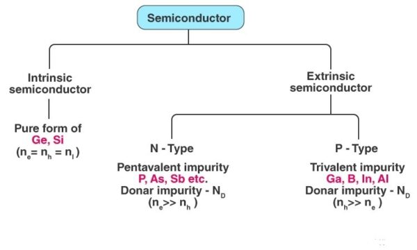
_
Difference Between Intrinsic and Extrinsic Semiconductors:
|
Intrinsic Semiconductor |
Extrinsic Semiconductor |
|
Pure semiconductor |
Impure semiconductor |
|
Density of electrons is equal to the density of holes |
Density of electrons is not equal to the density of holes |
|
Electrical conductivity is low |
Electrical conductivity is high |
|
Dependence on temperature only |
Dependence on temperature as well as on the amount of impurity |
|
No impurities |
Trivalent impurity, pentavalent impurity |
______
Doping:
The conductivity of semiconductors may easily be modified by introducing impurities into their crystal lattice. The process of adding controlled impurities to a semiconductor is known as doping. The amount of impurity, or dopant, added to an intrinsic (pure) semiconductor varies its level of conductivity. Doped semiconductors are referred to as extrinsic. By adding impurity to the pure semiconductors, the electrical conductivity may be varied by factors of thousands or millions.
A 1 cm3 specimen of a metal or semiconductor has the order of 1022 atoms. In a metal, every atom donates at least one free electron for conduction, thus 1 cm3 of metal contains on the order of 1022 free electrons, whereas a 1 cm3 sample of pure germanium at 20 °C contains about 4.2×10²² atoms, but only 2.5×10¹³ free electrons and 2.5×10¹³ holes. The addition of 0.001% of arsenic (an impurity) donates an extra 1017 free electrons in the same volume and the electrical conductivity is increased by a factor of 10,000.
The materials chosen as suitable dopants depend on the atomic properties of both the dopant and the material to be doped. In general, dopants that produce the desired controlled changes are classified as either electron acceptors or donors. Semiconductors doped with donor impurities are called n-type, while those doped with acceptor impurities are known as p-type. The n and p type designations indicate which charge carrier acts as the material’s majority carrier. The opposite carrier is called the minority carrier, which exists due to thermal excitation at a much lower concentration compared to the majority carrier.
Most ICs are made of silicon, which is abundant in ordinary beach sand. Pure crystalline silicon, as with other semiconducting materials, has a very high resistance to electrical current at normal room temperature. However, with the addition of certain impurities, known as dopants, the silicon can be made to conduct usable currents. In particular, the doped silicon can be used as a switch, turning current off and on as desired. The process of introducing impurities is known as doping or implantation. Depending on a dopant’s atomic structure, the result of implantation will be either an n-type (negative) or a p-type (positive) semiconductor. An n-type semiconductor results from implanting dopant atoms that have more electrons in their outer (bonding) shell than silicon. The resulting semiconductor crystal contains excess, or free, electrons that are available for conducting current. A p-type semiconductor results from implanting dopant atoms that have fewer electrons in their outer shell than silicon. The resulting crystal contains “holes” in its bonding structure where electrons would normally be located. In essence, such holes can move through the crystal conducting positive charges.
_
Semiconductor crystal used for IC etc. is high purity single crystal silicon of 99.999999999%, but when actually making a circuit, impurities are added to control the electrical properties. Depending on the added impurities, they become n-type and p-type semiconductors. In intrinsic crystalline silicon, there are approximately 5×10²² atoms/cm3. Doping concentration for silicon semiconductors may range anywhere from 1013/cm3 to 1018/cm3.
N-type semiconductors include phosphorus or arsenic. Both substances have five valence electrons. If a silicon atom is replaced by an atom with five outer electrons, such as arsenic, four of the electrons form covalent bonds with the four neighbouring silicon atoms. The fifth electron becomes a conduction electron that is donated to the conduction band, so it is available to allow electrical flow. The silicon becomes an n-type semiconductor because of the addition of the electron. Electrons have negative charges, so these semiconductors are called N-type semiconductors. When this free electron is attracted to the positive electrode and moves, current flows.
P-type semiconductors are “doped” with boron or gallium. The two doping elements have only three valence electrons. If an atom with three outer electrons, such as boron, is substituted for a silicon atom, an additional electron is accepted to form four covalent bonds around the boron atom, and a positively charged hole is created in the valence band. This creates a p-type semiconductor, with the boron constituting an acceptor. The lack of an electron creates a positive charge, so silicon doped with boron or gallium is called a P-type semiconductor. When a voltage is applied in this state, the neighboring electrons move to the hole, so that the place where an electron is present becomes a new hole, and the holes appear to move to the negative electrode in sequence.
An N-type semiconductor carries current mainly in the form of negatively charged electrons similar to the conduction of current in a wire. A P-type semiconductor carries current predominantly as electron deficiencies called holes. A hole has a positive electric charge, equal and opposite to the charge on an electron. In a semiconductor material, the flow of holes occurs in a direction opposite to the flow of electrons.
_____
P-N junction:
The contact surface between a p-type and an n-type semiconductor is called a P-N junction. A p-n junction is an interface or a boundary between two semiconductor material types, namely the p-type and the n-type, inside a semiconductor. The p-side or the positive side of the semiconductor has an excess of holes and the n-side or the negative side has an excess of electrons. If an abrupt change in impurity type from acceptors (p-type) to donors (n-type) occurs within a single crystal structure, a p-n junction is formed. On the p side, the holes constitute the dominant carriers and so are called majority carriers. A few thermally generated electrons will also exist in the p side; these are termed minority carriers. On the n side, the electrons are the majority carriers, while the holes are the minority carriers. Near the junction is a region having no free charge carriers. This region, called the depletion layer, behaves as an insulator.
The processes that follow after the formation of a p-n junction are of two types – diffusion and drift. As we know, there is a difference in the concentration of holes and electrons at the two sides of a junction, the holes from the p-side diffuse to the n-side and the electrons from the n-side diffuse to the p-side. These give rise to a diffusion current across the junction.
Also, when an electron diffuses from the n-side to the p-side, an ionized donor is left behind on the n-side, which is immobile. As the process goes on, a layer of positive charge is developed on the n-side of the junction. Similarly, when a hole goes from the p-side to the n-side, and ionized acceptor is left behind in the p-side, resulting in the formation of a layer of negative charges in the p-side of the junction. This region of positive charge and negative charge on either side of the junction is termed as the depletion region. So an electric field direction from a positive charge towards the negative charge is developed. Due to this electric field, an electron on the p-side of the junction moves to the n-side of the junction. This motion is termed as the drift. Here, we see that the direction of drift current is opposite to that of the diffusion current.
When the p-type is connected to the positive terminal of the battery and the n-type to the negative terminal then the p-n junction is said to be forward-biased. When the p-n junction is forward biased, the built-in electric field at the p-n junction and the applied electric field are in opposite directions. When both the electric fields add up, the resultant electric field has a magnitude lesser than the built-in electric field. This results in a less resistive and thinner depletion region. The depletion region’s resistance becomes negligible when the applied voltage is large. In silicon, at the voltage of 0.6 to 0.7 V, the resistance of the depletion region becomes completely negligible and the current flows across it unimpeded.
When the p-type is connected to the negative terminal of the battery and the n-type is connected to the positive side then the p-n junction is said to be reverse biased. In this case, the built-in electric field and the applied electric field are in the same direction. When the two fields are added, the resultant electric field is in the same direction as the built-in electric field creating a more resistive, thicker depletion region. The depletion region becomes more resistive and thicker if the applied voltage becomes larger. Almost no current flows.
The most important characteristic of p-n junctions is that they rectify. When a forward bias is applied to the p-n junction (i.e., a positive voltage applied to the p-side with respect to the n-side), the majority charge carriers move across the junction so that a large current can flow. However, when a reverse bias is applied, the charge carriers introduced by the impurities move in opposite directions away from the junction, and only a small leakage current flows. As the reverse bias is increased, the leakage current remains very small until a critical voltage is reached, at which point the current suddenly increases. This sudden increase in current is referred to as the junction breakdown, usually a nondestructive phenomenon if the resulting power dissipation is limited to a safe value. The applied forward voltage is typically less than one volt, but the reverse critical voltage, called the breakdown voltage, can vary from less than one volt to many thousands of volts, depending on the impurity concentration of the junction and other device parameters.
Although other junction types have been invented (including p-n-p and n-p-n), p-n junctions remain fundamental to semiconductor devices.
_
‘Doping’ is a procedure that makes semiconductors such as silicon and germanium ready for use in diodes and transistors. Semiconductors in their undoped form are actually electrical insulators that don’t insulate very well.
Putting an electron-doped semiconductor (n-type) with a hole-doped semiconductor (p-type) creates a diode. When p-type and n-type semiconductors are joined, the composite device (called p-n junction diode) produces the rectifier effect in which the flow of electric current is released or stopped depending on the direction of the electric field. A transistor is a semiconductor device used to amplify or switch electrical signals. The name transistor is a combination of the words transfer and resistor. Transistors were developed because, once the rectifier effect had been attained with semiconductors, people needed a semiconductor device for amplifying electrical signals for telegraph and telephone. A semiconductor is broadly defined today as a material with electrical conductivity that can be freely controlled by one means or another. In another words, whatever material that can be used as a transistor is a semiconductor. When integrated circuits are manufactured, thin component film is coated with a photo-resistant substance, onto which the circuit pattern is projected using photolithography technology, and then circuit components such as transistors and wiring are deposited on the surface of a thin silicon crystal wafer. This results in a single circuit layer, with transistors on the lowest level. The process is then repeated with many circuits formed on top of one another and the semiconductor base.
There was a time when germanium and silicon were exclusively used as semiconductors, and only the group 14 elements in the periodic table were deemed to be semiconductors. As studies on compound semiconductors and organic semiconductors progressed, however, the definition of a semiconductor also changed to include all kinds of semiconducting materials, rather than just a specific group of elements. Fairly recent additions to the category of semiconductors include carbon nanotubes discovered by Dr. Sumio Iijima, and conductive polymers discovered by Dr. Hideki Shiarakawa and others who won the Nobel Prize in Chemistry. Applications of these semiconductor materials are being studied by researchers around the world.
________
Speed in semiconductor:
Electrons can have a wide range of speeds:
A slow case: Electricity in your home is transfer of electrical energy as electromagnetic waves outside copper wires from source to load (appliance) generated by oscillation or movement of electrons in the copper wire. Electricity moves near speed of light but actual electrons are moving very slowly. We know that electrons move when there is a current flow in a wire, but the speed at which the electrons themselves move in the wire – the so-called electron drift velocity – surprises most people. For example, for a copper wire of radius 1 mm carrying a steady current of 10 Amps, the drift velocity is only about 0.024 cm/sec!
On the fast side: the Bohr model of the hydrogen atom has the (bound) electron zipping around the nucleus at about 2 million meters/sec.
And on the very fast side, some examples are: beta particles, which are emitted by some radioactive materials; and the innermost electrons of atoms of elements having large atomic number, such as Uranium. In these cases, the electrons are traveling near the speed of light. (About 180 million meters/sec).
What happens in chips?
The speed of electrons is thousands, up to millions of times faster inside transistors, when compared to the speed inside wires. In wires, the common electron-cloud (electron sea) is very dense due to one or two mobile electrons provided by every atom resulting in collision between them reducing speed while in semiconductors, few electrons are available and hence no collision and fast speed under effect of field. Charge Carrier mobility in semiconductors is doping dependent. In silicon (Si) the electron mobility is of the order of 1,000, in germanium around 4,000, and in gallium arsenide up to 10,000 cm2/ (V⋅s). Hole mobilities are generally lower and range from around 100 cm2/ (V⋅s) in gallium arsenide, to 450 in silicon, and 2,000 in germanium.
All current computer device technologies are indeed limited by the speed of electron motion. This limitation is rather fundamental, because the fastest possible speed for information transmission is of course the speed of light, and the speed of an electron is already a substantial fraction of this.
The ‘clock rate’ of a computer is limited by the maximum length that signals have to travel divided by the speed of light in the wires and by the size of transistors divided by the speed of electrons in silicon. The computer can be made faster by the simple expedient of decreasing its size. Better techniques for miniaturization have been for many years, and still are, the most important approach to speeding up computers.
______
Figure below depicts synopsis of semiconductor concepts:
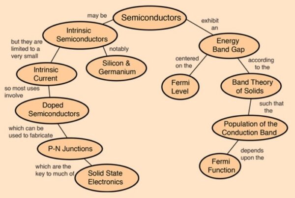
Semiconductors are employed in the manufacture of various kinds of electronic devices, including diodes, transistors, and integrated circuits. Such devices have found wide application because of their compactness, reliability, power efficiency, and low cost. As discrete components, they have found use in power devices, optical sensors, and light emitters, including solid-state lasers. They have a wide range of current- and voltage-handling capabilities and, more important, lend themselves to integration into complex but readily manufacturable microelectronic circuits. They are, and will be in the foreseeable future, the key elements for the majority of electronic systems, serving communications, signal processing, computing, and control applications in both the consumer and industrial markets.
Prior to the invention of the bipolar transistor in 1947, semiconductors were used only as two-terminal devices, such as rectifiers and photodiodes. During the early 1950s germanium was the major semiconductor material. However, it proved unsuitable for many applications, because devices made of the material exhibited high leakage currents at only moderately elevated temperatures. Since the early 1960s silicon has become by far the most widely used semiconductor, virtually supplanting germanium as a material for device fabrication. The main reasons for this are twofold: (1) silicon devices exhibit much lower leakage currents, and (2) silicon dioxide (SiO2), which is a high-quality insulator, is easy to incorporate as part of a silicon-based device. Thus, silicon technology has become very advanced and pervasive, with silicon devices constituting more than 95 percent of all semiconductor products sold worldwide.
Many of the compound semiconductors have some specific electrical and optical properties that are superior to their counterparts in silicon. These semiconductors, especially gallium arsenide, are used mainly for optoelectronic and certain radio frequency (RF) applications.
_______
Semiconductor Power Devices:
While semiconductors like the CPU and the LSI are used for computing and memory, power devices are used for electricity control and conversion. Speaking of semiconductor might imagine the IC. But power devices are semiconductors that can operate under large current and high voltage, in contrast to ICs. For example, the power circuit called an inverter that controls the electric power for running a train is embedded with power devices called a gate turn-off thyristor (GTO) and an insulated gate bipolar transistor (IGBT). These power devices turn the power on/off several hundred times to several tens of thousands times per second. In addition, these power devices can handle high voltage of several thousand volts, enabling the operation of the Shinkansen bullet train.
Inverters embedded with the efficient IGBT and other power devices are used in home appliances such as air conditioners, refrigerators, microwaves, rice cookers and LCD televisions, which are indispensable in our everyday live. They are also used in hybrid cars, fuel cells, solar cells and wind power generation, which are essential for taking measures against global warming. (Speaking of “inverter”, it often refers to the entire device which combined with the converter.)
_______
_______
Section-6
Chip materials:
The different types of semiconductors have slightly different properties and lend themselves to different applications in various forms of semiconductor devices. Some may be applicable for standard signal applications, others for high frequency amplifiers, while other types may be applicable for power applications and harsh environments or others for light emitting applications. All these different applications tend to utilise different types of semiconductor materials.
Semiconductor material groups:
Most commonly used semiconductor materials are crystalline inorganic solids. These materials are often classified according to their position or group within the periodic table. These groups are determined by the electrons in the outer orbit. Semiconductor materials are usually present in the group 14 of periodic table or also present as a combination of group 13 and group 15, or as a combination of group 12 and group 14 as well. While most semiconductor materials used are inorganic, a growing number of organic materials are also being investigated and used. The elemental semiconductors are those composed of single species of atoms, such as silicon (Si) and germanium (Ge) in group 14. There are, however, numerous compound semiconductors, which are composed of two or more elements.
Semiconductor materials list:
There are many different types of semiconductor materials that can be used within electronic devices. Each has its own advantages, disadvantages and areas where it can be used to offer the optimum performance.
|
Material |
Chemical Symbol |
Group |
Details |
|
Germanium |
Ge |
14 |
This type of semiconductor material was used in many early devices from radar detection diodes to the first transistors. Diodes show a higher reverse conductivity and temperature coefficient meant that early transistors could suffer from thermal runaway. Offers a better charge carrier mobility than silicon and is therefore used for some RF devices. Not as widely used these days as better semiconductor materials are available. |
|
Silicon |
S |
14 |
Silicon is the most widely used type of semiconductor material. Its major advantage is that it is easy to fabricate and provides good general electrical and mechanical properties. Another advantage is that when it is used for integrated circuits it forms high quality silicon oxide that is used for insulation layers between different active elements of the IC. |
|
Gallium arsenide |
GaAs |
13-15 |
Gallium arsenide is the second most widely used type of semiconductor after silicon. It is widely used in high performance RF devices where its high electron mobility is utilised. It is also used as substrate for other III-V semiconductors including indium gallium arsenide, aluminum gallium arsenide and others. However it is a brittle material and has a lower hole mobility than Silicon which makes applications such as P-type CMOS transistors not feasible. It is also relatively difficult to fabricate and this increases the costs of GaAs devices. |
|
Silicon carbide |
SiC |
14 |
Silicon carbide finds uses in a number of applications. It is often used in power devices where its losses are significantly lower and operating temperatures can be higher than those of silicon based devices. Silicon carbide has a breakdown capability which is about ten times that of silicon itself. Forms of silicon carbide were types of semiconductor material that were used with some early forms of yellow and blue LEDs. |
|
Gallium Nitride |
GaN |
13-15 |
This type of semiconductor material is starting to be more widely in microwave transistors where high temperatures and powers are needed. It is also being used in some microwave ICs. GaN is difficult to dope to give p-type regions and it is also sensitive to ESD, but relatively insensitive to ionising radiation. Has been used in some blue LEDs. |
|
Gallium phosphide |
GaP |
13-15 |
This semiconductor material has found many uses within LED technology. It was used in many early low to medium brightness LEDs producing a variety of colours dependent upon the addition of other dopants. Pure Gallium phosphide produces a green light, nitrogen-doped, it emits yellow-green, ZnO-doped it emits red. |
|
Cadmium sulphide |
CdS |
12-16 |
Used in photoresistors and also solar cells. |
|
Lead sulphide |
PbS |
14-16 |
Used as the mineral galena, this semiconductor material was used in the very early radio detectors known as ‘Cat’s Whiskers’ where a point contact was made with the tin wire onto the galena to provide rectification of the signals. |
_____
Compound semiconductors:
Compound semiconductors are typically constructed from two or more materials, which contain three or five electrons in their outer orbital, e.g., gallium (3) and arsenide (5) form gallium arsenide (GaAS). These semiconductors have a number of advantages over silicon chips, the first of which is their superior electrical properties. Some compound semiconductors can increase the speed at which electrons pass through them sixfold, allowing for faster processing speeds. Just as important, compound semiconductors have particularly strong photonic properties, allowing them to turn light into electricity and electricity into light highly efficiently. This makes them perfect for light-based communications like fiber optics. Photonics as a whole provides fertile ground for semiconductor growth due to the increasing importance of fiber optic broadband, complex cameras and light-based communication systems. Compound materials are expensive to produce compared to their silicon alternatives.
One solution is to layer compound semiconductors onto a silicon substrate, which reduces cost but leads to problems of its own. Silicon’s crystalline lattice does not work well with compound semiconductors. The resulting semiconductor contains faulty electron pathways due to the mismatch of both materials. The problem is not insurmountable. IBM is using a technique known as confined epitaxial lateral overgrowth to develop silicon compound hybrids. IQE uses its patented cREO technology instead, adding a buffer between the silicon and compound material to mitigate compatibility issues.
______
The most used semiconductor materials are silicon, germanium, and gallium arsenide. Of the three, germanium was one of the earliest semiconductor materials used. Germanium has four valence electrons, which are electrons located on the outer shell of the atom. The number of valence electrons in a semiconductor material determines its conductivity. While an important step in the evolution of semiconductor materials, germanium has largely fallen into disuse in favor of the current king of semiconductor materials—silicon.
Silicon has seen extensive use as a semiconductor material since the 1950s. The most abundant element on earth’s crust after oxygen, silicon has four valence electrons and melts at a higher temperature than germanium (1414 degrees Celsius in comparison to germanium’s 938.3 degrees Celsius). Silicon is abundantly available in quartzite. Extraction, purification, and crystallization processes for silicon are both efficient and economical. The element crystallizes in a diamond form for a relatively robust bond, giving silicon crystals strong mechanical properties.
Gallium arsenide is the second most common semiconductor in use today. Unlike silicon and germanium, gallium arsenide is a compound, not an element, and is made by combining gallium, with its three valence electrons, with arsenic, which has five valence electrons. Eight valence electrons make gallium-arsenide devices respond quickly to electric signals, making the compound well suited for amplifying the high-frequency signals seen in television satellites. Gallium arsenide has some limitations, however: the compound is more difficult to manufacture en masse than silicon, and the chemicals used in gallium arsenide production are quite toxic.
In addition to gallium arsenide, the compound silicon dioxide has characteristics superior to silicon, allowing it to be used as an insulator, passivation layer, and a building layer in metal-oxide silicon (MOS) devices, a type of insulated-gate field-effect transistor. Silicon dioxide has a high dielectric strength and wider band gap than silicon, making it an effective insulator, and the compound is easily deposited on other materials.
While the most important material in semiconducting manufacture for most of the late twentieth and early twenty-first centuries, silicon is reaching the limit of its usefulness. Demands for ever-smaller, faster integrated circuits have pushed the material’s efficiency about as far as it can go, with industry experts fearing silicon will soon reach the limits of Moore’s Law. Research into new materials is ongoing, with some materials holding great promise for the future:
-High-power gallium nitride could be used for more efficient, faster power conversions in electric grid systems due to its high critical energy field.
-Antimonide-based and bismuthide-based semiconductors are seeing use in improved infrared sensors for the medical and military sectors.
-Graphene has the potential to surpass silicon as an all-purpose semiconductor material, but widespread commercialization could be as long as twenty-five years away.
-Pyrite could be used to replace the rare earth element cadmium telluride, which is widely used in solar cells but which has a limited supply. Pyrite is abundant, inexpensive, and nontoxic
_____
_____
The semiconductor material silicon:
Semiconductors are widely used in familiar electric appliances such as personal computers, televisions, smartphones, digital cameras, IC cards, etc. The material most frequently used in semiconductors is Silicon (chemical symbol = Si). Silicon is the second most abundant element on earth after Oxygen. Most Silicon is found in soil and rock, but Silicon is also contained in natural water, trees and plants.
In nature, however, Silicon is found in the form of compounds with Oxygen, Aluminum and Magnesium. As a result, the Silicon element must be extracted from the compound and purified. Silicon used in a semiconductor such as an integrated circuits (IC) requires a single crystal structure of ultra-high-purity “99.999999999% (the so-called “eleven nines”) and is refined using various processes after extraction.
A single crystal structure is a structure whereby atoms are arranged in an orderly fashion in three dimensions, and the basic unit of the arrangement is called the crystal lattice. A single crystal is a crystal lattice in an orderly, continuous arrangement. A Silicon crystal lattice has a diamond cubic crystal structure in a repeating pattern of eight atoms. Each Silicon atom is combined with four neighboring silicon atoms by four bonds. Silicon, a very common element, is used as the raw material of semiconductors because of its stable structure.
Purification of Silicon consumes large amounts of power. In Japan, refined Silicon (ingot) with purity of at least 98% is imported from Australia, China and Brazil, where electricity is relatively inexpensive.
_
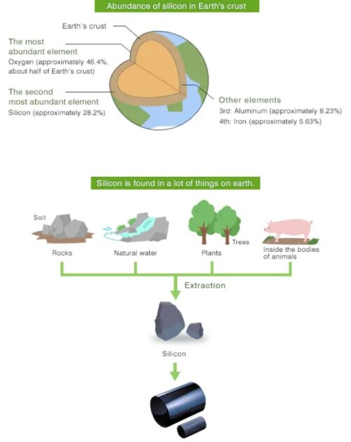
_
The small integrated circuits are usually built out of semiconducting materials such as quartz. Chips are made of sand, but not just any kind of sand. Scientifically speaking, the term “sand” is an expression of a certain grain size — 0.063 to 2 mm, to be precise.
Chips are made of silicon, which is a semiconductor, and in order to make the most efficient use of it, chip manufacturers use sand that contains as much silicon as possible. The mineral quartz is ideal for this purpose because its two main components are silicon and oxygen. Quartz is a very common mineral, present in many types of rock; and sand often has a high quartz content because it’s mostly pulverized rock.
In its pure form, quartz is a colourless mineral, which explains why many non-tropical beaches have white sand, but ordinary beach sand is unfit for the manufacturing of chips. The process requires sand with a very high quartz content from a rock called quartzite, which is made of 99 per cent pure quartz. These types of rocks are formed from sand that was squeezed together over time and heated deep in the Earth, so that almost all other elements have disappeared from the rock.
Figure below shows sand having high concentration of quartz.

Silicon (Si) is gathered typically from sand, which is mostly comprised of quartz particles (i.e., SiO2). Foundries can then extract the Si from the sand and through lots of purification processes, get highly pure Si (99.999999999%). Because SiO2 is so abundant on the Earth’s crust, it’s fairly cheap to get large volumes of highly pure Si.
_____
Preparation of semiconductor materials:
To create an ideal semiconducting material, chemical purity is paramount. Any small imperfection can have a drastic effect on how the semiconducting material behaves due to the scale at which the materials are used. A high degree of crystalline perfection is also required, since faults in the crystal structure (such as dislocations, twins, and stacking faults) interfere with the semiconducting properties of the material. Crystalline faults are a major cause of defective semiconductor devices. The larger the crystal, the more difficult it is to achieve the necessary perfection. Current mass production processes use crystal ingots between 100 and 300 mm (3.9 and 11.8 in) in diameter, grown as cylinders and sliced into wafers.
There is a combination of processes that are used to prepare semiconducting materials for ICs. One process is called thermal oxidation, which forms silicon dioxide on the surface of the silicon. This is used as a gate insulator and field oxide. Other processes are called photomasks and photolithography. This process is what creates the patterns on the circuit in the integrated circuit. Ultraviolet light is used along with a photoresist layer to create a chemical change that generates the patterns for the circuit.
The etching is the next process that is required. The part of the silicon that was not covered by the photoresist layer from the previous step can now be etched. The main process typically used today is called plasma etching. Plasma etching usually involves an etch gas pumped in a low-pressure chamber to create plasma. A common etch gas is chlorofluorocarbon, or more commonly known Freon. A high radio-frequency voltage between the cathode and anode is what creates the plasma in the chamber. The silicon wafer is located on the cathode, which causes it to be hit by the positively charged ions that are released from the plasma. The result is silicon that is etched anisotropically.
The last process is called diffusion. This is the process that gives the semiconducting material its desired semiconducting properties. It is also known as doping. The process introduces an impure atom to the system, which creates the p–n junction. To get the impure atoms embedded in the silicon wafer, the wafer is first put in a 1100 degree Celsius chamber. The atoms are injected in and eventually diffuse with the silicon. After the process is completed and the silicon has reached room temperature, the doping process is done and the semiconducting material is ready to be used in an integrated circuit.
_______
Various Materials in Chips:
Chips have three materials that contribute to the bulk of their designs — silicon, plastic and copper. Silicon dioxide comes from either silica sand or from quartz. The silicon requires purification. To produce silicon from quartz, producers melt and crystalize the rock. The created crystals are so strong that they require the use of a diamond saw to cut them into thin wafers. Sand requires a similar number of steps to produce the electronic grade silicon ingots.
Typically, these purified cylindrical ingots of silicon are 12 inches across and have a purity of 99.999999999%, or one foreign particle per one billion silicon atoms. The wafers or ingots may require storage and transport to get to chip producing factories, which must maintain intensely clean atmospheres to prevent contamination of the chips. In fact, chip production cleanrooms require cleanliness 1,000 times higher than sterile hospital operating rooms.
However, some minerals used in smaller amounts are just as important in the function of the chips and processors. For example, to clean off the silicon wafers and ensure their purity, manufacturers use hydrogen peroxide and sulfuric acid. A rinse of hydrofluoric acid and deionized water follows a pair of baths in these first two chemicals. Lastly, the wafers undergo a final bath in hydrochloric acid, hydrogen peroxide and deionized water.
Other materials some manufacturers may use in their chips include the following:
Hafnium: A rare metal used most often in nuclear reactors. It speeds up CPUs.
Potassium hydroxide: This chemical, also known as caustic potash, etches a circuit design onto the board.
Gold: Gold is used in printed circuit boards, cell phones, computer chips (CPU), connectors and fingers.
Silver: Silver is used in printed circuit boards, cell phones, computer chips, keyboard membranes and some capacitors.
Platinum: Platinum is used in hard drives and circuit boards components.
Palladium: Palladium is used in cell phones, hard drives, circuit board components and capacitors.
Copper: Copper is used in CPU heat sinks, wiring cables, cell phones, printed circuit boards and computer chips.
Nickel: Nickel is used in to circuit board components.
Tantalum: Tantalum is used in circuit board components and some capacitors.
Cobalt: Cobalt is included hard drives.
Aluminum: Aluminum is used in printed circuit boards, computer chips, hard drive, CPU heat sinks.
Tin: Tin is used in printed circuit boards and computer chips.
Zinc: Zinc is used in printed circuit boards.
Neodymium: Neodymium is used in hard drives.
These are only some of the numerous materials used in producing chips. Some chemicals used during the processing or the precious metals require careful handling due to their dangerous nature or expense. Safe transport and storage of these materials are crucial elements of the supply chain for computer and electronics manufacturers.
____
Storage of Chip Materials:
Though many manufacturers order materials on demand to cover gaps in the supply chain, makers such as Texas Instruments, often keep about 90 days of inventory available to fulfill needs. Chemicals need careful temperature and environmentally controlled conditions to protect them from spilling or causing damage due to their caustic nature. You must protect wafers and dies from electrostatic discharge (ESD) and temperature extremes. Whether you store the dies and wafers out of their protective nitrogen-filled bags determines the storage conditions. When kept sealed inside their bags, maintain similar temperatures as you would during shipping and a humidity level around 75%. If you remove wafers or dies from their bags, keep them in a sealed container of nitrogen gas. Humidity must remain between 7% and 30%. Keep the inside of these containers between 18 degrees Celsius (64.4 degrees Fahrenheit) and 24 degrees Celsius (75.2 degrees Fahrenheit). Refrigerated container units can help you to keep such a tightly restricted storage environment for either wafers and dies either in their bags or out of their nitrogen-filled transportation bags.
______
______
Why silicon used in Electronics as a Semiconductor Material?
With the term ‘electronics’, there are many things you can associate, especially the electronic circuit board components like transistors, diodes, ICs and so on. If you are completely aware of these components, you must be aware of the prevailing silicon uses in the manufacturing of these components as well. Silicon is a semiconductor material with an atomic number of 14, located in the group 14 of the periodic table. Pure Amorphous silicon was first prepared by Jones Jacob Berzelius in 1824, whereas crystalline silicon was first prepared by Henry Etienne in 1854. Semiconductors are nothing but materials with insulating properties in pure form and conducting properties when doped or added with impurities. Semiconductors usually have a band gap (energy required for electrons to break free from covalent bond) between insulators (maximum band gap) and conductors (minimum band gap). The conduction or flow of charge in semiconductors is due to the movement of free electrons or holes. The most widely used semiconductors are Silicon, Germanium and Gallium-Arsenide.
What makes Silicon as the most preferred semiconductor material in electronics?
Silicon is brilliant. Brilliant because it’s a natural semiconductor—able to both conduct electricity and act as an insulator, depending on the conditions—and because it can be engineered at small scale. Brilliant because it is the second-most-common element on Earth, probably clinging to the soles of your feet right now, and easily produced by heating sand. Those attributes have made it the bedrock of virtually every technology we use today. Engineers spend their time thinking about how to pack more silicon into less space—an exponential march from thousands of transistors per chip in the 1970s to billions today. With Moore’s law, we are swimming in silicon.
The following are the top most reasons:
-1. Abundance of Silicon
The foremost and most prominent reason for silicon’s popularity as a material of choice is its abundance. Next in line with oxygen which is about 46% in the earth’s crust, Silicon forms about 28% of the earth’s crust. It is widely available in the form of sand (silica), and quartz. The most readily available source of silicon is sand. But the silicon, which is obtained from sand, is not pure enough at the very first stage, it cannot be used as it is for manufacturing products since it contains 0.5% of impurities. It might sound like 99.5% purity is cool, but processors need 99.999999999% purity. Such silicon is called electronic, and it can be obtained after passing a chain of certain chemical reactions.
-2. Cost
Silicon is the second most abundant element on Earth, behind only oxygen. It can be extracted from sand relatively easily. This availability, combined with the ease of creating circuits with silicon, makes it very inexpensive to produce, especially compared to other semiconductors. Gallium is better than silicon but its cost of extraction, manufacture, and production would make it unfeasible to make it a substitute for the element that is much more abundant. Gallium arsenide has certain technical advantages over silicon – electrons race through its crystalline structure faster than they can move through silicon. But silicon has a crushing commercial advantage. It is roughly a thousand times cheaper to make.
-3. Silicon manufacturing techniques are effective and economic
The silicon wafers that are used for the production of ICs and electronic components are manufactured using effective and economical techniques. Various processes facilitate the achievement of required diameter, orientation, conductivity, doping concentration and oxygen concentration needed for the production of silicon wafers.
-4. Suitable Atomic Structure & properties
The physical properties of Silicon contribute to its popularity and usage as a semiconductor material. Almost all processors that are manufactured in the world are silicon-based due to the fact that silicon has a suitable internal atomic structure, which allows microcircuits and processors to be made in almost any configuration. Crystalline Silicon used mostly in electronics, consists of a diamond like structure. Each unit cell consists of 8 atoms in a bravais lattice arrangement. This makes pure silicon highly stable at room temperature when compared to other materials like Germanium. Thus, pure silicon is least affected by water, acid or steam. Also, at higher temperature in a molten state, silicon easily forms oxides and nitrides and even alloys.
Conventionally at room temperature, the energy bandgap for Silicon is 1.12 eV and that of Germanium is 0.7 eV. This makes silicon a stable element when compared to Germanium and reduces the chance of leakage current. The reverse current is in nano-amperes and is very low. Si has a very nice bandgap of ~ 1.12 eV, not too high so that room temperature can’t ionize it, and not so low that it has to high leakage current.
Crystalline structure of Silicon consists of face centric cubic lattice structure with 34% packing density. This allows easy substitution of impurities’ atoms in the empty places of the lattice. In other words, doping concentration is quite high. This also enhances the possibility of adding impurities like oxygen as the interstitial atoms within the crystal lattice. This provides a strong mechanical strength to the wafers against different kinds of stresses like thermal, mechanical or gravitational.
Forward voltage for silicon diodes is 0.7 V, which is higher when compare to Germanium diodes. This makes them more stable and enhances silicon uses as rectifiers. The knee voltage for Si is around 0.7 volts, unlike the germanium (~0.3Volts) it won’t go ON quickly. So the advantage in this is, suppose if you have some kind of source that can’t produce exactly 0 volt for Ground conditions, rather, it fluctuates 0.2–0.3 volts, now if you were using germanium then you might end up getting unwanted “ON Switch” conditions.
-5. Stability
Silicon remains very stable after alloying processes. This allows manufacturers to produce materials like semiconductors, circuits, or insulators. Silicon is highly reliable and enhances certain aspects when using it in CPUs.
Silicon can also withstand higher temperatures; it is thermally stable up to 1100°C which is a very favourable quality of elements for the industries as the fabrication and manufacturing processes may involve higher temperatures (oxidation is achieved at high temperature).
-6. Ease
Unlike other semiconductors, silicon’s conductivity is very easy to change. Through the doping process, manufacturers can introduce elements that make silicon more conductive, less conductive, and even non-conductive. As a result, manufacturers can use fewer materials for chips and make more intricate circuits for increased function. It is easy to remove impurities and easy to purify silicon.
-7. Gate material
It forms a very nice gate material. Most modern FET’s used in VLSI (up until the latest generations) have been called MOSFET and have used Si as the gate material. Basically the success of Si is the success of MOSFET, which with scaling and extreme integration has driven the industry. MOSFET’s are not so easily manufactured in other material systems, and you can’t drive the same level of integration in other semiconductors.
-8. Silicon carbide
Semiconductors with wide band gap imply materials with the band gap energy above 2 eV. Those semiconductors are suitable for high power electronics, high temperature, and high operation frequency conditions. The Silicon Carbide (SiC) gives the best results in commercial electronic components production. It has band gap energy of 3.26 eV. SiC is a compound semiconductor composed of silicon and carbide. SiC provides a number of advantages over silicon, including 10x the breakdown electric field strength, 3x the band gap, and enabling a wider range of p- and n-type control required for device construction.
-9. Silicon nitride
It forms a very tough Nitride, Si3N4 Silicon Nitride forms a very high bandgap insulator which is impermeable. – this is used to passivate (seal) the die; and this also used to make hard masks and in other process steps.
-10. Silicon Dioxide (SiO2)
The last but not the least reason for the huge popularity of silicon, is the ease with which it forms oxides. In most transistor designs, a highly insulating material is needed to reduce electron current leakage. In the early days of semiconductor based computers, the fabrication people struggled a lot with semiconductors like Germanium because they could not grow a highly insulating material on the Germanium surface. Eventually they found that Si naturally oxidizes to form SiO2, getting the insulator they needed essentially for free. It forms an oxide that is of very high quality, seals the surface with very few pin holes or gap, and this allows MOSFET to be more easily made as the SiO2 forms the insulating layer for the Gate. SiO2 has been called the chip designer’s friend. Silicon dioxide is the most widely used insulator in IC technology owing to its extremely stable chemical nature when compare to other oxides like Germanium, which is water soluble and decomposes at a temperature of 800 degree Celsius.
Silicon dioxide is used:
-In IC fabrication techniques like etching, diffusion, ion implantation, etc.
-In Dielectrics for the electronic devices.
-As an Ultrathin layer for MOS and CMOS devices. This has in fact increased the wide popularity of CMOS devices with high input impedance.
-In 3D devices in MEMs technology.
______
Why is carbon not a semiconductor although it is in the same group as silicon and germanium?
Carbon does exhibit semiconductor property but it will require a lot of energy to work. The more an electron is near to the nucleus, the stronger is the covalent bond. Since carbon has only 2 shells, the valence electrons are pretty tightly bonded, while in case of silicon, its ideal i.e., 3 shells. Germanium is not a preferred semiconductor and is used in very few applications because the valence electrons are so loosely coupled that it starts conduction even at room temperature.
Also, Semiconductor classification is made based on the energy gap or band gap energy. Materials with energy gap 0.1eV to 3.5eV are known as semiconductors. Carbon which has 5.5eV band gap doesn’t come under this category. It is high band gap material.
______
______
Section-7
Silicon to semiconductor to diode to transistor to chip to PCB:
_
Silicon to semiconductor:
Today, most semiconductor chips and transistors are created with silicon. You may have heard expressions like “Silicon Valley” and the “silicon economy,” and that’s why — silicon is the heart of any electronic device. Silicon is a very common element — for example, it is the main element in sand and quartz. If you look “silicon” up in the periodic table, you will find that it sits next to aluminum, below carbon and above germanium. Carbon, silicon and germanium (germanium, like silicon, is also a semiconductor) have a unique property in their electron structure — each has four electrons in its outer orbital. This allows them to form nice crystals. The four electrons form perfect covalent bonds with four neighboring atoms, creating a lattice. In carbon, we know the crystalline form as diamond. In silicon, the crystalline form is a silvery, metallic-looking substance.
In a silicon lattice, all silicon atoms bond perfectly to four neighbors, leaving no free electrons to conduct electric current as seen in the figure below. This makes a silicon crystal an insulator rather than a conductor.
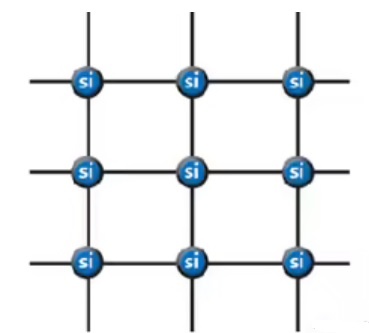
Metals tend to be good conductors of electricity because they usually have “free electrons” that can move easily between atoms, and electricity involves the flow of electrons. While silicon crystals look metallic, they are not, in fact, metals. All of the outer electrons in a silicon crystal are involved in perfect covalent bonds, so they can’t move around. A pure silicon crystal is nearly an insulator — very little electricity will flow through it.
You can change the behavior of silicon and turn it into a conductor by doping it. In doping, you mix a small amount of an impurity into the silicon crystal.
There are two types of impurities:
N-type – In N-type doping, phosphorus or arsenic is added to the silicon in small quantities. Phosphorus and arsenic each have five outer electrons, so they’re out of place when they get into the silicon lattice. The fifth electron has nothing to bond to, so it’s free to move around. It takes only a very small quantity of the impurity to create enough free electrons to allow an electric current to flow through the silicon. N-type silicon is a good conductor. Electrons have a negative charge, hence the name N-type.
P-type – In P-type doping, boron or gallium is the dopant. Boron and gallium each have only three outer electrons. When mixed into the silicon lattice, they form “holes” in the lattice where a silicon electron has nothing to bond to. The absence of an electron creates the effect of a positive charge, hence the name P-type. Holes can conduct current. A hole happily accepts an electron from a neighbor, moving the hole over a space.
A minute amount of either N-type or P-type doping turns a silicon crystal from a good insulator into a viable (but not great) conductor — hence the name “semiconductor.”
____
Semiconductor to diode:
The p-n junction (vide supra):
A p-type or an n-type semiconductor is not very useful on its own. However, joining these opposite materials creates what is called a p-n junction. A p-n junction forms a barrier to conduction between the materials. Although the electrons in the n-type material are attracted to the holes in the p-type material, the electrons are not normally energetic enough to overcome the intervening barrier. However, if additional energy is provided to the electrons in the n-type material, they will be capable of crossing the barrier into the p-type material—and current will flow. This additional energy can be supplied by applying a positive voltage to the p-type material. The negatively charged electrons will then be highly attracted to the positive voltage across the junction.
A barrier forms along the boundary between p-type and n-type semiconductors that is known as a p-n junction. Because electrons under ordinary conditions will flow in only one direction through such barriers, p-n junctions form the basis for creating electronic rectifiers and switches.
Adding a small primary voltage such that the electron source (negative terminal) is attached to the n-type semiconductor surface and the drain (positive terminal) is attached to the p-type semiconductor surface results in a small continuous current. This arrangement is referred to as being forward-biased.
A p-n junction that conducts electricity when energy is added to the n material is called forward-biased because the electrons move forward into the holes. If voltage is applied in the opposite direction—a positive voltage connected to the n side of the junction—no current will flow. The electrons in the n material will still be attracted to the positive voltage, but the voltage will now be on the same side of the barrier as the electrons. In this state a junction is said to be reverse-biased. Since p-n junctions conduct electricity in only one direction, they are a type of diode. Diodes are essential building blocks of semiconductor switches.
N-type and P-type silicon are not that amazing by themselves; but when you put them together, you get some very interesting behavior at the junction. That’s what happens in a diode.
A diode is the simplest possible semiconductor device, and is therefore an excellent beginning point if you want to understand how semiconductors work. A diode allows current to flow in one direction but not the other. You may have seen turnstiles at a stadium or a subway station that let people go through in only one direction. A diode is a one-way turnstile for electrons.
_
When you put N-type and P-type silicon together as shown in diagram below, you get a very interesting phenomenon that gives a diode its unique properties.
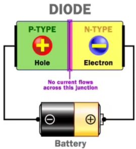
Even though N-type silicon by itself is a conductor, and P-type silicon by itself is also a conductor, the combination shown in the diagram does not conduct any electricity. The negative electrons in the N-type silicon get attracted to the positive terminal of the battery. The positive holes in the P-type silicon get attracted to the negative terminal of the battery. No current flows across the junction because the holes and the electrons are each moving in the wrong direction.
If you flip the battery around, the diode conducts electricity just fine. The free electrons in the N-type silicon are repelled by the negative terminal of the battery. The holes in the P-type silicon are repelled by the positive terminal. At the junction between the N-type and P-type silicon, holes and free electrons meet. The electrons fill the holes. Those holes and free electrons cease to exist, and new holes and electrons spring up to take their place. The effect is that current flows through the junction.
_____
Diodes to Junction Transistors:
A device that blocks current in one direction while letting current flow in another direction is called a diode. Diodes can be used in a number of ways. For example, a device that uses batteries often contains a diode that protects the device if you insert the batteries backward. The diode simply blocks any current from leaving the battery if it is reversed — this protects the sensitive electronics in the device. Diode is useful if you want to turn alternating (two-way) electric current into direct (one-way) current. Diodes can also be made so they give off light when electricity flows through them. You might have seen these light-emitting diodes (LEDs) on pocket calculators and electronic displays on hi-fi stereo equipment.
When reverse-biased, an ideal diode would block all current. A real diode lets perhaps 10 microamps through — not a lot, but still not perfect. And if you apply enough reverse voltage (V), the junction breaks down and lets current through. Usually, the breakdown voltage is a lot more voltage than the circuit will ever see, so it is irrelevant.
When forward-biased, there is a small amount of voltage necessary to get the diode going. In silicon, this voltage is about 0.7 volts. This voltage is needed to start the hole-electron combination process at the junction.
Another monumental technology that’s related to the diode is the transistor. Transistors and diodes have a lot in common.
Place the N-type and P-type adjacent to each other and you create a P-N diode. This diode allows an electrical current to flow, but in only one direction, a useful property in the construction of electronic circuits.
Full-fledged transistors were the next step. To create transistors, engineers layered doped semiconductor to make two layers back to back, in a configuration of either P-N-P or N-P-N. You can create either an NPN or a PNP sandwich. In a way, a transistor is just a pair of interconnected diodes. The point of contact was called a junction, thus the name junction transistor.
With small electrical current applied to the center layer (called the base), electrons will move from the N-type side to the P-type side. The initial small trickle acts as a switch that allows much larger current to flow. In an electric circuit, this means that transistors are acting as both a switch and an amplifier.
A transistor looks like two diodes back-to-back. You’d imagine that no current could flow through a transistor because back-to-back diodes would block current both ways. And this is true. However, when you apply a small current to the center layer of the sandwich, a much larger current can flow through the sandwich as a whole. This gives a transistor its switching behavior. A small current can turn a larger current on and off.
When transistor works as an amplifier, it takes in a tiny electric current at one end (an input current) and produces a much bigger electric current (an output current) at the other. Transistors can also work as switches. A tiny electric current flowing through one part of a transistor can make a much bigger current flow through another part of it. In other words, the small current switches on the larger one. This is essentially how all computer chips work.
A silicon chip is a piece of silicon that can hold thousands of transistors. With transistors acting as switches, you can create Boolean gates, and with Boolean gates you can create microprocessor chips.
_
Field-effect transistors:
Bringing a negative voltage close to the centre of a long strip of n-type material will repel nearby electrons in the material and thus form holes—that is, transform some of the strip in the middle to p-type material. This change in polarity using an electric field gives the field-effect transistor its name. While the voltage is being applied, there will exist two p-n junctions along the strip, from n to p and then from p back to n. One of the two junctions will always be reverse-biased. Since reverse-biased junctions cannot conduct, current cannot flow through the strip.
The field effect can be used to create a switch (transistor) to turn current off and on, simply by applying and removing a small voltage nearby in order to create or destroy reverse-biased diodes in the material. A transistor created by using the field effect is called a field-effect transistor (FET). The location where the voltage is applied is known as a gate. The gate is separated from the transistor strip by a thin layer of insulation to prevent it from short-circuiting the flow of electrons through the semiconductor from an input (source) electrode to an output (drain) electrode.
Similarly, a switch can be made by placing a positive gate voltage near a strip of p-type material. A positive voltage attracts electrons and thus forms a region of n within a strip of p. This again creates two p-n junctions, or diodes. As before, one of the diodes will always be reverse-biased and will stop current from flowing.
FETs are good for building logic circuits because they require only a small current during switching. No current is required for holding the transistor in an on or off state; a voltage will maintain the state. This type of switching helps preserve battery life. A FET is called unipolar (from “one polarity”) because the main conduction method is either holes or electrons, not both.
Enhancement-mode FETs:
There are two basic types of FETs. The type described previously is a depletion-mode FET, since a region is depleted of its natural charge. The field effect can also be used to create what is called an enhancement-mode FET by enhancing a region to appear similar to its surrounding regions.
An n-type enhancement-mode FET is made from two regions of n-type material separated by a small region of p. As this FET naturally contains two p-n junctions—two diodes—it is normally switched off. However, when a positive voltage is placed on the gate, the voltage attracts electrons and creates n-type material in the middle region, filling the gap that was previously p-type material. The gate voltage thus creates a continuous region of n across the entire strip, allowing current to flow from one side to the other. This turns the transistor on. Similarly, a p-type enhancement-mode FET can be made from two regions of p-type material separated by a small region of n. The gate voltage required for turning on this transistor is negative. Enhancement-mode FETs switch faster than depletion-mode FETs because they require a change only near the surface under the gate, rather than all the way through the material.
Complementary metal-oxide semiconductors:
Recall that placing a positive voltage at the gate of an n-type enhanced-mode FET will turn the switch on. Placing the same voltage at the gate of a p-type enhanced-mode FET will turn the switch off. Likewise, placing a negative voltage at the gate will turn the n-type off and the p-type on. These FETs always respond in opposite, or complementary, fashion to a given gate voltage. Thus, if the gates of an n-type and a p-type FET are connected any voltage applied to the common gate will operate the complementary pair, turning one on and leaving the other off. A semiconductor that pairs n- and p-type transistors this way is called a complementary metal-oxide semiconductor (CMOS). Because complementary transistor pairs can quickly switch between two logic states, CMOSs are very useful in logic circuits. In particular, because only one circuit is on at any time, CMOSs require less power and are often used for battery-powered devices, such as in digital cameras, and for the special memory that holds the date, time, and system parameters in personal computers.
Bipolar transistors:
Bipolar transistors simultaneously use holes and electrons to conduct, hence their name (from “two polarities”). Like FETs, bipolar transistors contain p- and n-type materials configured in input, middle, and output regions. In bipolar transistors, however, these regions are referred to as the emitter, the base, and the collector. Instead of relying, as FETs do, on a secondary voltage source to change the polarity beneath the gate (the field effect), bipolar transistors use a secondary voltage source to provide enough energy for electrons to punch through the reverse-biased base-collector junction. As the electrons are energized, they jump into the collector and complete the circuit. Note that even with highly energetic electrons, the middle section of p-type material must be extremely thin for the electrons to pass through both junctions.
A bipolar base region can be fabricated that is much smaller than any CMOS transistor gate. This smaller size enables bipolar transistors to operate much faster than CMOS transistors. Bipolar transistors are typically used in applications where speed is very important, such as in radio-frequency ICs. On the other hand, although bipolar transistors are faster, FETs use less current. The type of switch a designer selects depends on which benefits are more important for the application: speed or power savings. This is one of many trade-off decisions engineers make in designing their circuits.
_____
Transistor to systems:
In the analog world of continuously varying signals, a transistor is a device used to amplify its electrical input. Audio amplifiers use transistors in this manner.
In the digital world, a transistor is a binary switch and the fundamental building block of computer circuitry. Like a light switch on the wall, the transistor either prevents or allows current to flow through. A single modern CPU can have hundreds of millions or even billions of transistors.
In a digital circuit, a transistor is an on/off switch that is conductive when pulsed with electricity. Transistors are wired in patterns that make up logic gates. Gates make up circuits, and circuits make up electronic systems (IC/chip) as seen in the figure below:
![]()
The natural progression from silicon to doped silicon to transistors to chips is what has made microprocessors and other electronic devices so inexpensive and ubiquitous in today’s society. The fundamental principles are surprisingly simple. The miracle is the constant refinement of those principles to the point where, today, tens of millions of transistors can be inexpensively formed onto a single chip.
_
Transistor vs. resistor vs. capacitor:
A transistor is a semiconductor device used to amplify or switch electrical signals and power. The transistor is one of the basic building blocks of modern electronics. It is composed of semiconductor material, usually with at least three terminals for connection to an electronic circuit. Transistor is a solid-state semiconductor device, with three terminals, which can be used for amplification, switching, voltage stabilization, signal modulation, and many other functions.
The name transistor is a contraction of “transfer resistor”. Of course, the transistor can be used as a resistor that is exactly what it is – a controllable resistance. The resistance is between the collector and emitter – we control it by applying suitable signals to the base.
A resistor has the ability to reduce voltage and current when used in a circuit. The main function of a resistor is to limit current flow. A diode needs a resistor in series to limit the current. Without it, it is hardly possible to adjust the current through the diode in a way the diode can be operated correctly.
Transistors function much in the same way variable resistors do. The difference is that you can control the resistance of a transistor by applying current. As such, we often use transistors in conjunction with a pull-up resistor or pull-down resistor. Inversely, variable resistors require manual analog switching.
A capacitor is (electronics) an electronic component capable of storing an electric charge; especially one consisting of two conductors separated by a dielectric. It generally opposes changes in current in electrical and electronic circuits.
Modern random-access memory (RAM) uses MOS field-effect transistors (MOSFETs) as flip-flops, along with MOS capacitors for certain types of RAM. The SRAM (static RAM) memory cell is a type of flip-flop circuit, typically implemented using MOSFETs. Dynamic Random Access Memory, DRAM is constructed using capacitors and a few transistors. In this type of RAM, the capacitor is used for storing the data where bit value, which signifies that the capacitor is charged and a bit value 0, which means that the capacitor is discharged.
SRAM consists of flip-flops, a bistable circuit composed of four to six transistors. Once a flip-flop stores a bit, it keeps that value until the opposite value is stored in it. DRAM, the most common type of RAM in consumer computers, is made up of capacitors. Non-volatile memory, like a flash drive, is not made of capacitors as they lose their charge soon after a power source is removed.
______
Overview of computer system:
-1. Matter is composed of atoms.
-2. Atoms have electrons and flow of these electrons under influence of voltage generates current.
-3. Semiconductor’s conductivity can be increased and controlled by doping with impurities and gating with electric fields.
-4. Semiconductors are put together in a particular way to create transistors.
-5. Now, to make use of electrons, we create transistors which can store/free electricity as needed. They are stored in units of 1 (5Volts) and 0 (0 Volts).
-6. Transistors are put together in a particular way to create logic gates.
-7. Logic gates are put together in a particular way to create registers, counters, adders, etc – the various logic components within a CPU for example. By assembling logic gates, you can create an ALU that can do computations.
-8. The logic components within a CPU are put together in a particular way to create the CPU itself. An organization of registers and memory makes CPU+RAM
-9. The CPU is combined with other components in a computer in a particular way to make the computer hardware itself.
-10. The computer operating system is put together in a particular way to operate the computer hardware.
-11. Software is designed in a particular way to use the operating system functions to perform everything that you can do with a computer.
-12. To make it easy to compute using the CPU, we developed machine code. This language is what essentially runs on the CPU. Machine code, also known as machine language, is the elemental language of computers. It is read by the computer’s central processing unit (CPU), is composed of digital binary numbers and looks like a very long sequence of zeros and ones.
-13. An assembly language is a type of low-level programming language that is intended to communicate directly with a computer’s hardware. Unlike machine language, which consists of binary and hexadecimal characters, assembly languages are designed to be readable by humans.
______
Central Processing Unit (CPU):
The CPU is the brain of a computer, containing all the circuitry needed to process input, store data, and output results. The CPU is constantly following instructions of computer programs that tell it which data to process and how to process it. Without a CPU, we could not run programs on a computer. For example, a simple calculator program might instruct the CPU to take two numbers, 2 and 2, add them, and send back the result.
The CPU can process those instructions easily, thanks to a control unit that knows how to interpret program instructions and an Arithmetic Logic Unit (ALU) that knows how to add numbers. With the control unit and ALU combined, the CPU can process much more complex programs than a simple calculator.
Inside the CPU:
At the hardware level, a CPU is an integrated circuit, also known as a chip. An integrated circuit “integrates” millions or billions of tiny electrical parts, arranging them into circuits and fitting them all into a compact box.
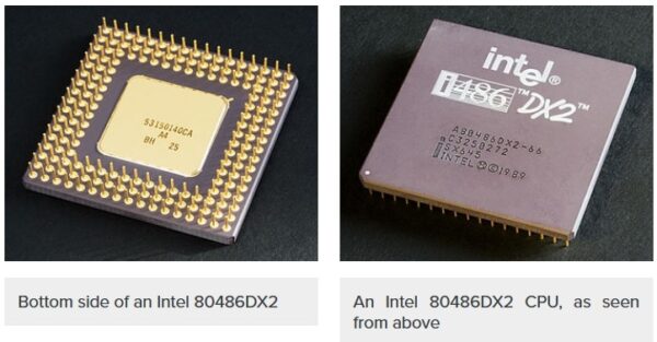
A central processing unit (CPU) is the electronic circuitry within a computer that carries out the instructions of a computer program by performing the basic arithmetic, logical, control and input/output (I/O) operations specified by the instructions. The term has been used in the computer industry at least since the early 1960s. Traditionally, the term “CPU” refers to a processor, more specifically to its processing unit and control unit (CU), distinguishing these core elements of a computer from external components such as main memory and I/O circuitry. The processor is a chip or a logical circuit that responds and processes the basic instructions to drive a particular computer. The main functions of the processor are fetching, decoding, executing, and write back the operations of an instruction. The processor is also called the brain of any system which incorporates computers, laptops, smartphones, embedded systems, etc.
The form, design and implementation of CPUs have changed over the course of their history, but their fundamental operation remains almost unchanged. Principal components of a CPU include the arithmetic logic unit (ALU) that performs arithmetic and logic operations, processor registers that supply operands to the ALU and store the results of ALU operations, and a control unit that fetches instructions from memory and “executes” them by directing the coordinated operations of the ALU, registers and other components.
Most modern CPUs are microprocessors, meaning they are contained on a single integrated circuit (IC) chip. An IC that contains a CPU may also contain memory, peripheral interfaces, and other components of a computer; such integrated devices are variously called microcontrollers or systems on a chip (SoC). Some computers employ a multi-core processor, which is a single chip containing two or more CPUs called “cores”; in that context, single chips are sometimes referred to as “sockets”. Array processors or vector processors have multiple processors that operate in parallel, with no unit considered central.
_
We can visualize the layers of the CPU chip stacked from bottom to top as seen in the figure below. At the bottom is transistor and wire, then logic gate, then logic circuit, and then a chip.
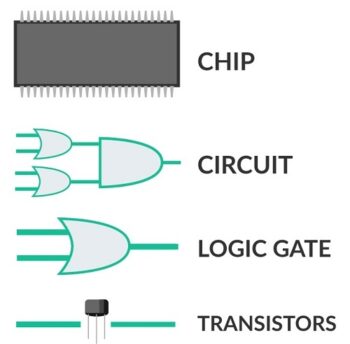
Some of those layers are physical devices, like the chip and transistors, and some of those layers are abstractions, like logic circuits and gates. In fact, transistors and wires are fabricated on silicon die and packed as a chip.
It’s impressive that we can put together seemingly simple devices like logic gates to create CPUs that power complex devices like our phones, computers, and even self-driving cars.
_
CPU speed (clock speed):
A computer’s processor clock speed determines how quickly the central processing unit (CPU) can retrieve and interpret instructions. This helps your computer complete more tasks by getting them done faster. Clock speeds are measured in gigahertz (GHz), with a higher number equating to higher clock speed. Multi-core processors were developed to help CPUs run faster as it became more difficult to increase clock speed. Faster clock speeds mean that you’ll see tasks ordered from your CPU completed quicker, making your experience seamless and reducing the time you wait to interface with your favorite applications and programs.
In general, a higher clock speed means a faster CPU. However, many other factors come into play. Your CPU processes many instructions (low-level calculations like arithmetic) from different programs every second. The clock speed measures the number of cycles your CPU executes per second, measured in GHz (gigahertz). During each cycle, billions of transistors within the processor open and close. A CPU with a clock speed of 3.2 GHz executes 3.2 billion cycles per second. Sometimes, multiple instructions are completed in a single clock cycle; in other cases, one instruction might be handled over multiple clock cycles. Since different CPU designs handle instructions differently, it’s best to compare clock speeds within the same CPU brand and generation. For example, a CPU with a higher clock speed from five years ago might be outperformed by a new CPU with a lower clock speed, as the newer architecture deals with instructions more efficiently. While CPU speed is important, you must also consider how it can work with your cores and how that may affect your computing experience. These two aspects of your CPU should be evaluated together to determine whether or not your computer is running at optimum speed.
_____
AI chips:
Artificial intelligence will play an important role in national and international security in the years to come. As a result, the U.S. government is considering how to control the diffusion of AI-related information and technologies. Because general-purpose AI software, datasets, and algorithms are not effective targets for controls, the attention naturally falls on the computer hardware necessary to implement modern AI systems. The success of modern AI techniques relies on computation on a scale unimaginable even a few years ago. Training a leading AI algorithm can require a month of computing time and cost $100 million. This enormous computational power is delivered by computer chips that not only pack the maximum number of transistors—basic computational devices that can be switched between on (1) and off (0) states—but also are tailor-made to efficiently perform specific calculations required by AI systems. Such leading-edge, specialized “AI chips” are essential for cost-effectively implementing AI at scale; trying to deliver the same AI application using older AI chips or general-purpose chips can cost tens to thousands of times more.
AI chips include graphics processing units (GPUs), field-programmable gate arrays (FPGAs), and application-specific integrated circuits (ASICs) that are specialized for AI. General-purpose chips like central processing units (CPUs) can also be used for some simpler AI tasks, but CPUs are becoming less and less useful as AI advances. Like general-purpose CPUs, AI chips gain speed and efficiency (that is, they are able to complete more computations per unit of energy consumed) by incorporating huge numbers of smaller and smaller transistors, which run faster and consume less energy than larger transistors. But unlike CPUs, AI chips also have other, AI-optimized design features. These features dramatically accelerate the identical, predictable, independent calculations required by AI algorithms. They include executing a large number of calculations in parallel rather than sequentially, as in CPUs; calculating numbers with low precision in a way that successfully implements AI algorithms but reduces the number of transistors needed for the same calculation; speeding up memory access by, for example, storing an entire AI algorithm in a single AI chip; and using programming languages built specifically to efficiently translate AI computer code for execution on an AI chip.
Because of their unique features, AI chips are tens or even thousands of times faster and more efficient than CPUs for training and inference of AI algorithms. State-of-the-art AI chips are also dramatically more cost-effective than state-of-the-art CPUs as a result of their greater efficiency for AI algorithms. An AI chip a thousand times as efficient as a CPU provides an improvement equivalent to 26 years of Moore’s Law-driven CPU improvements.
______
______
Power of Transistors:
A transistor is a tiny device that either switches electric current on and off or amplifies an electric current. The original transistors were small cylinders, a bit larger than a pencil eraser. Over the years, scientists and engineers have been able to make transistors tinier and tinier. With the invention of the integrated circuit, or microchip, in which thousands or millions of transistors are deposited on a piece of silicon, transistors have become microscopic. Transistors are devices that control the movement of electrons, and consequently, electricity. They work something like a water faucet — not only do they start and stop the flow of a current, but they also control the amount of the current. With electricity, transistors can both switch or amplify electronic signals, letting you control current moving through a circuit board with precision.
Transistors are the main component of the microchips used in computers. Computers operate on a binary system, which uses only two digits: 0 and 1. In a computer microchip, transistors act as switches, letting current through to represent the binary digit 1, or cutting it off to represent 0. Every kind of information (words, numbers, pictures, etc.) are converted into strings of 1s and 0s. The simple switch operation of transistors is what enables your computer to complete massively complex tasks. In a computer chip, transistors switch between two binary states — 0 and 1. This is the language of computers. One computer chip can have millions of transistors continually switching, helping complete complex calculations. An integrated circuit is one piece of semiconductor material loaded with transistors and other electronic components. Computers use those currents in tandem with Boolean algebra to make simple decisions. With many transistors, a computer can make many simple decisions very quickly, and thus perform complex calculations very quickly, too. Computers need millions or even billions of transistors to complete tasks. Thanks to the reliability and incredibly small size of individual transistors, which are much smaller than the diameter of a single human hair, engineers can pack an unfathomable number of transistors into a wide array of computer and computer-related products.
Today many household appliances including televisions, VCRs, stereos, telephones, refrigerators, washers and dryers, microwave ovens, alarm systems, and fax machines have chips built into them. The chips allow the devices to process great volumes of information and provide the user with exactly the information desired, from identifying the name and phone number of a caller to playing and replaying the chorus of the latest hip-hop release.
Transistors are also found in pacemakers, hearing aids, cameras, calculators, and watches. Most of these devices draw their power from tiny batteries. Most spacecraft also rely on microchips, and thus transistors. The transistor is truly the “nerve cell” of the information age.
_
In the 1960s and 1970s, transistorized products mostly used the fundamental junction transistor design developed by Bell Labs. Advances in silicon development in the 1970s led to metal oxide semiconductor field effect transistors (MOSFET). MOSFETs utilize the same principles as other transistors, but the N- and P-types of silicon are less expensive, are arranged differently and are doped with other types of metals and oxides, depending on the intended use.
There are many other transistor types, too. Engineers categorize transistors by their semiconductor material, application, structure, power ratings, operating frequencies and other variables. As technology advanced, engineers learned that they could manufacture many transistors simultaneously, on the same piece of semiconductor material, along with other components like capacitors and resistors.
The result is what’s called an integrated circuit. These circuits, usually called just “chips,” contain billions of infinitesimal transistors. Since the 1960s, the number of transistors per unit area has been doubling every 2 years, meaning engineers can cram more of them into smaller and smaller products.
Modern silicon commercial transistors may be smaller than 45 nanometers in size. They’re so small that NVDIA’s new graphics card (codenamed GF100) has more than 3 billion transistors, the most ever jammed into one chip. And these transistors are behemoths compared to what’s coming in the future.
Now it’s all about introducing new materials, new structures, new innovations. It’s about innovation, not scaling. At a physical level, we still want to make things smaller, but how we do that requires very different concepts and ideas at more fundamental and materials level… it used to be more [about] geometry.
Scientists from Yale and South Korea recently created the world’s first molecular transistor, which is made from a single benzene molecule. Although the tiny size is amazing, engineers stress that they’re not concerned so much with bulk as they are efficiency. Contemporary chips create a lot of wasted heat because their transistors don’t pass along energy as efficiently as product makers would like; molecular transistors may hold the key to improving efficiency in big ways.
Transistor materials are changing, too, thanks to recent advances in a material called graphene. Graphene transfers electrons much faster than silicon, and could lead to computer processors that are 1,000 times faster than silicon-based products.
No matter where development goes, it’s certain that transistors will continue to drive product research and technological advances we can’t yet even begin to imagine. Computers will become faster, cheaper and more reliable. Cell phones and music players will shrink to super-tiny dimensions, and still cost less than previous models.
That’s the power of transistors in altering the landscape of technology, and ultimately, of our society as a whole.
_____
_____
Printed Circuit Board (PCB):
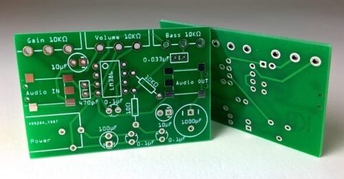
Printed circuit boards (PCBs) are the foundational building block of most modern electronic devices. Whether simple single layered boards used in your garage door opener, to the six layer board in your smart watch, to a 60 layer, very high density and high-speed circuit boards used in super computers and servers, printed circuit boards are the foundation on which all of the other electronic components are assembled onto. Semiconductors, connectors, resistors, diodes, capacitors and radio devices are mounted to, and “talk” to one another through the PCB. Conventional PCB’s can be as simple as a single layer of circuitry or can go to fifty layers or more. They consist of electrical components and connectors linked via conductive circuits – usually copper, with the purpose of routing electrical signals and power within and between devices.
PCB’s have mechanical and electrical attributes that make them ideal for these applications. Most PCBs manufactured in the World are rigid, roughly 90% of the PCB’s manufactured today are rigid boards. Some PCBs are flexible, allowing the circuits to be bent and folded into shape, or sometimes they are used where the flexible circuit will survive hundreds of thousands of flex cycles, without any break in the circuits. These flexible PCB’s comprise roughly 10% of the market. A small subset of these types of circuits are called rigid flex circuits, where one part of the board is rigid – ideal for mounting and connecting components, and one or more parts are flexible, providing the advantages of flexible circuits.
_
Open up a television or a radio and you’ll see it’s built around a printed circuit board (PCB): a bit like an electric street-map with small electronic components (such as transistors, resistors and capacitors) in place of the buildings and printed copper connections linking them together like miniature metal streets.
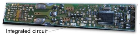
Figure above shows integrated circuit (right) on a printed circuit board (PCB) with various conventional electronic components.
_
Compared to traditional wired circuits, PCBs offer a number of advantages. Their small and lightweight design is appropriate for use in many modern devices, while their reliability and ease of maintenance suit them for integration in complex systems. Additionally, their low cost of production makes them a highly cost-effective option. These qualities are some of the reasons PCBs find application across industries and markets including medical, aerospace, military and commercial sectors.
A rapidly emerging PCB technology, separate from the ones above, is called printed electronics – typically very simple, very low cost, circuits that reduce electronic packaging expense to the level that electronic solutions can be developed to solve problems never considered before. They are often used in electronics for wearable applications, or disposable electronic devices – opening many opportunities for creative electrical designers.
______
_______
Section-8
Applications of Semiconductors Devices:
Semiconductors in everyday life:
Semiconductors are used in almost all electronic devices. Without them, our life would be much different and difficult. Their reliability, compactness, low cost and controlled conduction of electricity make them ideal to be used for various purposes in a wide range of components and devices. Transistors, diodes, photosensors, microcontrollers, integrated chips and much more are made up of semiconductors. Semiconductor manufacturing provides the foundational hardware for almost all electronic devices. It is used for amplification of energy, switching, energy conversion, sensors, and more. For example, temperature sensors used in air conditioners are made with semiconductors. Rice cookers cook rice perfectly because semiconductors control the temperature precisely. CPUs that operate personal computers are also made with semiconductors. Many digital consumer products in everyday life such as mobile phones / smartphones, digital cameras, televisions, washing machines, refrigerators and LED bulbs also use semiconductors.
In addition to consumer electronics, semiconductors play a central role in the operation of bank ATMs, trains, the internet, communications and other parts of social infrastructure, such as the medical network used for the care of elderly, among other things. Furthermore, efficient logistics systems help save energy and promote the preservation of the global environment. The number of car-mounted semiconductor devices has been increasing steadily. There are many types of car-mounted semiconductors. Particularly for future ADAS (Advanced Driver Assistance Systems), more semiconductors are expected to be used. In this way, semiconductors help us to live comfortable lives.
_
Sectors that are especially reliant on semiconductor materials include the following:
artificial intelligence
clean energy
communication
computing
energy
health care
Internet of Things
military
_
Types of Semiconductor Devices:
Electronic parts using semiconductors are called semiconductor devices.
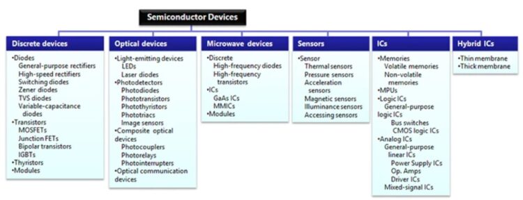
Many kinds of semiconductor devices have been developed in line with the expansion of application fields and the progress of electronic equipment. “Discrete semiconductors” are single devices with a single function, such as transistors and diodes. “Integrated circuits (ICs)” are devices with multiple functional elements mounted on one chip. Typical ICs include memories, microprocessors, and logic ICs. LSIs raised the degree of integration of ICs. Classification by general function/structure is shown above.
_
Semiconductor uses:
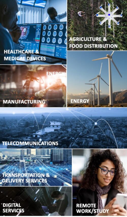
Microchips are used in many electrical devices besides a computer. In the 1960s, the Air Force used microchips to build the Minuteman II missile. NASA purchased microchips for its Apollo project. Today, microchips are used in smartphones that allow people to use the internet and have a telephone video conference. Microchips are also used in televisions, GPS tracking devices, identification cards as well as medicine, for the speedier diagnosis of cancer and other diseases.
__
All modern electronic products, such as televisions, cellphones, computers, cameras, washing machines, and microwaves, use integrated circuits (ICs). Microprocessors, oscillators, filters, and regulators are all examples of integrated circuits. Rugged integrated circuits are microchips that are engineered and developed to perform activities in harsh environments. Mixed ICs are a combination of analogue and digital ICs, resulting in superior integrated technology. Furthermore, depending on the manufacturing method or methodology, integrated circuits are available in a wide variety of products. Thin and thick film ICs, monolithic ICs, and hybrid or multichip ICs are some of the examples of these ICs. The robust integrated circuit is widely utilised in industries such as aerospace and defence, automotive, power, mining and metals, healthcare, and others.
Before the popular silicon-based chips came to be, computers were big machines made of tubes and dials. They were impressive but fragile, not to mention a liability because of the amount of electricity they needed. Semiconductor chips replaced the tubes, managing machines faster, cheaper, and more efficiently. Advances in design and size led us to light and sleek modern phones and smart equipment in a range of industries. The global chip shortage highlights the importance of semiconductor chips and why restoring and increasing their production is essential to modern living.
Here are the sectors and industries that revolve around semiconductor chips.
-1. Computing
Microchips and computers are usually the first connection people make. Depending on the type of chip, a semiconductor uses binary code to direct the commands you give it, whether it’s to launch a program or download and save a document. Microprocessors (CPUs), memory, and graphic processing units (GPUs) are common semiconductors for computers. All-in-all, they help your machine run smoothly, for example, by protecting your battery and whole system from burning up while you play video games.
-2. Telecommunication
The principle of semiconductors for telecommunication is the same: to control machine functions. The difference is the types of chips used and what they’re used for. At the same time, their design differs from device to device. A smartphone’s semiconductor chips affect its display, navigation, battery use, 4G reception, and more. Even taking pictures and using different apps taps into one chip or another. But it’s not just about phones. Consider routers, answering machines, and pagers. The range of technologies that depend on telecommunication semiconductors really is broad.
-3. Household Appliances
Fridges, microwaves, washing machines, air conditioners, and other machines around the home and office operate thanks to semiconductors. Different chips control temperatures, timers, automated features, and so on. Our spaces are already full of appliances to make everyday habits easier, while smart technology and the Internet of Things (IoT) add to them. As a result, semiconductor chips constantly evolve to respond to rising standards, mainly demanding instant, multifunctional, and durable services.
-4. Banking
Once you understand what semiconductors can do, it’s easier to imagine how different parts of our high-tech world benefit from them. Banks are major investors, especially in the best microchips manufacturers have to offer. Computers and their banking systems for online communication, digital accounting, cloud platforms, and more are key. But banks also need semiconductors for ATMs, security cameras, and even automated locking mechanisms. This is also a case where the more powerful the technology, the better. Semiconductor chips can help banks keep your money and personal information safe, even more so as AI and machine learning evolve within banking.
-5. Security
When it comes to security, semiconductors have both improved and hindered it. The evolution of microchips alongside many other parts of digital technology has opened the way to new and intelligent threats. However, these same innovations also help defend against them. A semiconductor chip’s contribution to cybersecurity starts from the hardware. The effectiveness of any programs you install later depends on how well your machine supports them. For example, quality semiconductors in a camera with motion detection could allow faster alerts and security measures.
-6. Healthcare
The medical field uses advanced technology. Complex and risky surgeries are safer with the help of machines, operating with precision. Monitors and pacemakers are popular too. Even talking to patients and diagnosing symptoms is possible through video conferencing alone. And none of this equipment can do its job right without semiconductor chips directing the power, sensors, temperatures, pressures, calculations, and many other functions. Just like with security, a lot of care goes into designing the parts for medical devices and ensuring they don’t malfunction. Healthcare is an area where achievements in semiconductor technology shine the most. They improve our quality of life while safeguarding it too.
Examples of Medical Devices that rely on Semiconductor Technology are depicted in the figure below:
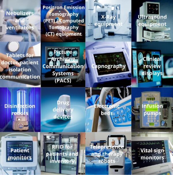
-7. RFID Tags
RFID tags are thought to be the ID cards of the future, potentially containing substantial amounts of data in simple encrypted text files. They are commonly proposed for a more streamlined health-care database in which a simple universal card or tag can be updated by any physician or health-care entity to build up a complete health history of a patient. Currently, these chips are used to track wild animals, and in some circumstances, household pets.
-8. Transportation
Cars, buses, trains, and planes are just much bigger devices that also use semiconductors. If you value GPS, free Wi-Fi, or the polite voice alerting you about each stop, then you can appreciate how these tiny but wonderful chips enhance everyday habits. In general, electronic vehicles have more features than analog models. They take the stress out of travel and replace it with a smooth experience and handy tools for navigation, roadside assistance, parking, and more. It’s because semiconductors are so widespread today that manufacturers need to focus on specific industries. Aviation is another major interest, enjoying super-efficient cockpit avionics, engine control systems, and power conversion, among other functions.
-9. Manufacturing
The benefits of semiconductors come full circle to improve their own manufacturing and that of every other commercial product. Machines in factories do specific and repetitive work, the result of carefully set up hardware and software. Also, keep in mind that each device draws on a certain amount of electricity. A bad design could short-circuit a part of the manufacturing process, causing delays and unnecessary expenses. So, whether a device is self-sufficient or needs someone to control it, its abilities must be trustworthy, which largely depends on its semiconductor chips. Several practical and economic factors are linked to a business’s trouble-free operation and production.
-10. Military
Advanced semiconductors play an important role in the defense industry. Semiconductors for commercial and military applications are not necessarily mutually exclusive. Electronic components in sophisticated military systems use many of the same logic and memory chips that appear in consumer electronics. For example, field-programmable gate arrays (FPGAs) are frequently used in military systems due to their low-cost and high modularity. However, there are military-specific requirements that call for semiconductors with certain features. While commercial chip production is heavily driven by cost and timely, large-scale production, the defense sector’s demand for chips emphasizes performance. Namely, military-specific chips must be more durable and reliable, have a higher heat tolerance, and in some cases, be radiation tolerant. As such, many military-specific chips contain compound semiconductors, which have superior electronic properties such as high electron mobility and direct band gap compared to silicon-only based semiconductors. Specifically, gallium arsenide (GaAs) and gallium nitride (GaN)-based chips appear most frequently in military-specific applications. Radio-frequency integrated circuits (RFICs) and monolithic microwave integrated circuits (MMICs) use GaAs and GaN technologies for a wide range of defense and aerospace uses. These include electromagnetic spectrum operations, signals intelligence, military communications, space capabilities, radars, jammers, and more.
Semiconductors are fundamental to the operation of virtually every military system, including communications and navigations systems and complex weapons systems such as those found in the F-35 Joint Strike Fighter. They are key to the ‘must-win’ technologies of the future, including artificial intelligence and 5G, which will be essential to achieving the goal of a dynamic, inclusive and innovative national economy. In addition, the development of advanced autonomous systems, cybersecurity, space and hypersonics, and directed energy is also dependent on semiconductor technologies.
_____
_____
Chips in car:
Did you know that a modern, medium-sized car contained up to 1,400 computer chips?
I did not.
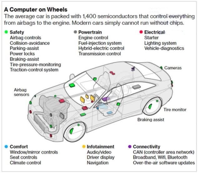
The average car is packed with 1,400 semiconductors that control everything from airbags to the engine. This number is going to increase further because of the development of self-driving cars and the trend away from a combustion engine towards electric vehicles. Cars and trucks have something like 100 distinct electronics modules, and each module has multiple chips. Wiring in cars is expensive and vulnerable, so it is better to distribute the information processing rather than run a bunch of wires back to one central processor. A typical car today has around 50 microcontrollers. Luxury automobiles may have a hundred or more. These microcontrollers are distributed throughout the vehicle, connected via a bus such as CAN or LIN. They are mostly low-cost microcontrollers, running without an operating system. However the main “Infotainment” system may use a more powerful microprocessor running Linux or other OS. The production of a semi-conductor takes six weeks to three months, depending on the features.
_
The electronics has become the tail that wags the automotive dog – – electronics have gone from being just 18% of a car’s cost in 2000, to being 40% of its cost in 2020, and projected to be 45% by 2030.
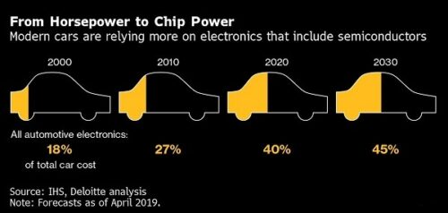
______
______
Role of Semiconductors in corona virus pandemic:
Semiconductors are the “brains” of electronic devices crucial to pandemic response and recovery of the global economy. They provide user input, display, wireless connectivity, processing, storage, power management, and other essential functions to a wide array of essential products, life-saving equipment and critical infrastructure. This includes healthcare and medical devices, telecommunications, energy, finance, transportation, agriculture, manufacturing, aerospace and defense. Semiconductors also underpin the IT systems that make remote work possible and provide access to essential services across every domain, including medicine, finance, education, government, food distribution, and more.
Throughout this global pandemic, semiconductor-rich devices have become increasingly prevalent in developing solutions for numerous problems in the economic and public health sphere. Semiconductors are an integral component of many medical devices used in hospitals and doctors’ offices today, including many devices that are critical to treating COVID-19 patients. Any medical device that can be plugged into an electric socket or has batteries depends on semiconductors to operate. Semiconductors provide functions such as operations control, data processing and storage, input and output management, sensing, wireless connectivity and power management. By enabling functions previously performed by non-semiconductor devices, semiconductors have often lowered costs and improved performance at the same time. This has proved critical to the COVID-19 response and improving health care in general.
______
______
Section-9
Chip implant:
A microchip implant is a small electronic circuit which is designed to be implanted into the body. The circuit is usually covered in a housing which will not react with the body or break down with use, protecting the chip inside for the lifetime of the wearer. A wide variety of information can be encoded on the microchip, ranging from data about allergies to identifying information. Microchip implants have not been without controversy, especially among people who are concerned about the potential for government tracking of human beings.
Microchip implants were first used in animals. An animal microchip implant can be used in a pet to ensure that the animal can be identified even if it loses its collar and tags, and microchips can also be used to identify and manage livestock, along with animals such as racehorses. Human microchip implants for medical use have been released by several companies, and some researchers have also experimented with microchip implants which interact with the environment, such as a chip which communicates with a computer to turn lights on and off.
Whether in a human or animal, a microchip implant works in the same way. The chip is about the size of a grain of rice, and it is typically equipped with RFID technology. Using a reader which is held over the site of the implant, someone can gather the information on the chip. Some can be written to by a reader/writer, while others must be programmed before insertion. Due to concerns about RFID security, some are encoded so that the information on the chip is secure.
Many are designed to be inserted with a large-bore needle which injects the microchip into the site, with this practice being standard for veterinary implants. Others are large enough that a surgical procedure must be used to implant the chip.
From a biological standpoint, one of the major problems with a microchip implant is that it is difficult to build chips which will remain stable in the body for a prolonged period. Sometimes chips are rejected by the body, and in other cases, they are corroded by body fluids. Glass-encased implants are inert, but the glass could break, potentially posing a very serious health risks. Biomedical researchers have worked on a number of microchip implant designs which are designed to address these problems.
There are numerous applications, including rapid identification where security is important, the use of prosthetic limbs and allowing deaf people to hear and blind people to see, and tracking pets and children or a person with dementia or a criminal on probation.
Ethicists have also expressed concerns about microchip implants. Some of these concerns revolve around the insecurity of RFID technology, with the potential for the harvesting of personal data from implants with the use of a device which can gather information from RFID transmitters. Other people have expressed concerns that microchipping of humans is an ethically questionable practice which could set the stage for government monitoring or other potentially sinister uses which have not been specified.
______
______
ID microchip implant in animals:
The ID microchip is a small glass capsule containing a special antenna. That antenna is encoded with a unique identification number. When a scanner emits the correct low-power radio frequency, the signal bounces back from the antenna modified to reflect that number. There is no power source in the chip, and the chip contains no actual information about that animal. Technically, it’s an RFID (Radio Frequency IDentification) device.
There are assigned implant locations for every species, from birds to elephants to snakes. Zoos typically chip every animal – this is proof of ownership.
The format of the number typically indicates the manufacturer who maintains their own database, cross-referencing the chip number with owner and pet registration. This is one reason to make sure you register with the manufacturer of your pet’s chip. Sure, many databases claim they can register any chip, but nobody will know to check their database.
_
Figure below depicts pet microchip:
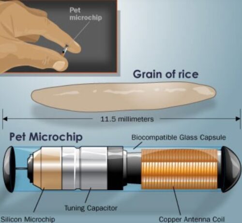
A pet microchip is about the size of a grain of rice. It consists of a tiny computer chip housed in a special type of glass. The main part is the microchip itself, which is connected to a tuning capacitor and a copper coil (antenna). RFID chip is an integrated circuit (IC). When the coil receives a small pulse of electromagnetic energy from a scanner, it transfers that energy into the capacitor, which activates the chip to send its information back to the scanner. The rest of the time, the chip is completely inert. That’s why they last all through the animal’s lifetime; they don’t even need an internal power source.
All of these components are encased in a capsule of bio-safe (sterile and nontoxic) glass, which may be coated with a substance called bio-bond that effectively glues it in place after a while. The whole device is not much larger than a grain of rice, and the animal won’t even notice it after the initial implantation.
_
To activate a microchip, a low-frequency field of about 125kHz is generated. This provides power to the microchip via transformer coupling and an activation code (modulated on the 125kHz). The microchip will wake up and, if it sees the activation code, will then send its stored data. The reader then looks at the data retrieved and determines whether it’s in the right format, after which it then does whatever it needs to do, such as unlocking a door, updating a database, etc. Each microchip contains a registration number and the phone number of the registry for the particular brand of chip. A handheld scanner reads the radio frequency of the chip and displays this information. An animal shelter or vet clinic that finds your pet can contact the registry to get your name and phone number. Up to 8 million animals end up in shelters every year. Unfortunately, only 15-20% of dogs and less than 2% of cats are ever reclaimed by their owners. One of the ways to increase the chances of finding your lost pet is having it microchipped. Microchips are a permanent, and the most reliable, method of identification. In fact, microchipped dogs are more than twice as likely to be returned to their owners, and microchipped cats are more than 20 times as likely to be returned to their owners.
_
How pet microchip is used:
-About the size of a grain of rice, a microchip contains a personal identification number that stays with your animal forever.
-The microchip is inserted under the skin of your animal with an injection and it is a safe and easy procedure.
-A microchip is not a GPS tracking device. The location of a lost animal cannot be tracked or determined from the microchip.
-The technology inside a microchip is the same as bar codes found on thousands of products we use every day. It is similar the grocery store being able to scan the bar code on a food item, and then information showing up on the cash register screen. Here it will show a series of numbers and letters that is unique to your animal’s record.
-When a lost animal is found, he/she can be taken to a local animal shelter, veterinary office, or animal control agency and examined with a hand-held scanner that reads the number specific to your animal. That unique code is connected to your name and contact information.
-To read the microchip’s bar code, a hand-held scanner is used. The scanner can only be used when the animal is physically present, and only shelters, veterinarians and animal control officers have this type of scanner.
-Once the microchip has been read, a phone call to the microchip manufacturer allows us to find out who the animal is registered to so that the process of reuniting the lost pet with their family begins.
-Most microchip manufacturers also maintain a national registration database with a telephone hotline.
_
Why microchip pet if he/she already wears a collar and tag?
Collars can fall off or break, tags can be lost or wear off so they are illegible. A combination of a microchip, properly fitting collar and current identification tag, and keeping your pet properly confined, are the best insurance policies you can provide to keep your pet safe. An added benefit: In many communities, the cost of a pet license is reduced when the cat or dog is also microchipped. Microchipping has multiple benefits. Millions of pets get lost and end up in shelters every year, but a microchipped dog can easily be reunited with owners.
______
______
Chip implant in humans:
Defense Advanced Research Projects Agency (DARPA), an agency of the United States Department of Defense, has developed cyborg insects that can transmit information from sensors implanted into the insect during the pupal stage. The insect’s motion is controlled from a micro-electro-mechanical system (MEMS), and it can be used to survey an environment or, say, detect explosives and poisonous gases. Similar high-value and path-breaking work using cutting-edge implantable technology is being done on humans, too.
Implants for humans are not new today. Installation of pacemakers and other medical innovations for prosthesis in humans are common and now basic procedures. Recently, microchip implants are embedded inside the human body, acting as unique lifetime identifiers. A human microchip implant is any electronic device implanted subcutaneously (subdermally) usually via an injection. Examples include an identifying integrated circuit RFID device encased in silicate glass which is implanted in the body of a human being. This type of subdermal implant usually contains a unique ID number that can be linked to information contained in an external database, such as identity document, criminal record, medical history, medications, address book, and other usage. The RFID microchip is basically a tiny, two-way radio, roughly the size of a grain of rice, capable of storing digital information. This technology makes it possible, among other things, to instantly verify and confirm the identity of a person. An RFID implant is capable of holding all the information usually carried on visiting cards. It can transmit this information as one walks through a security checkpoint.
_
A classic example is VeriChip tag, which contains a numerical code as identifier, readable from a distance of 10cm or less using a handheld reader. When illuminated by a low-frequency magnetic field (134kHz) generated by the reader, the tag powers up and transmits a unique 16-digit code, which can be used for identifying individuals remotely. With the pinch of a syringe, the microchip is inserted under the skin in a procedure that takes less than 20 minutes and leaves no stitches. Silently and invisibly, the dormant chip stores a code that releases patient-specific information when a scanner passes over it. The Chip itself contains no medical records, just codes that can be scanned, and revealed, in a doctor’s office or hospital. With that code, the health providers can unlock that portion of a secure database that holds that person’s medical information, including allergies and prior treatment. The electronic database, not the chip, would be updated with each medical visit. In pets, installing the chip runs about $50. For humans, the chip implantation cost would be $150 to $200.
Recent developments in technology have made possible new potential applications for RFID devices implanted in the human body. These can now be used for remote identification of persons, remotely controlling human biological functions, transmitting measurements of chemical or biological data inside the body, and monitoring biological activity or physiological functions of humans. The technology is not yet fully developed for real-time tracking of people using an implanted microchip. To be able to track anywhere on Earth, a GPS-controlled device would be required for this application. This would mean dimensions that are too large for implanting inside a human body.
_
Benefits of using microchip implants in humans:
The microchip implant can become a very useful tool, especially in emergency situations where instant access to the right medical information can mean the difference between life and death. Here are the various advantages of using implants.
-1. Easy accessibility to medical history
Implanted microchips are useful for patients, particularly those suffering from diabetes, cardiovascular disease or Alzheimer’s disease. The implanted microchip can be used in medical emergencies, especially when a patient is unconscious, to quickly gain access to his/her medical history, such as antibiotics taken in the past, allergies, medication regularly taken and other information that is relevant. The microchip itself need not contain the patient’s entire medical history, but rather a unique code that can be used to access the information from a database.
-2. Easy identification
Passports, driver’s license and so on, which are often used for identification purposes, are increasingly containing microchips. For example, passengers can be identified at an airport by scanning the microchip in their passports. It would require minimal changes in infrastructures at airports, and train and bus stations, to transit from scanned passports to scanned implanted chips. People would be identified easily just by walking past a reader.
-3. Institutional memberships and access control
Implanted microchips are convenient and practical to use in workplaces, hotels, gyms and anywhere else where identification is needed to grant access and make payments. Baja Beach Clubs in Rotterdam, Netherlands and Spain use implanted microchips for members, to avoid long waiting time in lines and for easy access to membership features and facilities. Members can keep track of what they have ordered. The computer automatically debits their bank account by scanning the chips, thus making the process of making payment convenient and easy.
-4. Easy tracking of persons
This is useful for keeping tabs on persons such as patients, children and criminals. For example, it is possible for babies to get mixed up at hospitals, for children to get lost in a crowd, run away from home or be kidnapped, for the elderly or hospital patients to wander out of care facilities, or for criminals to escape from prisons. In such instances, it is vital to be able to track people to provide peace of mind to millions of caregivers, family members, parents and relevant authorities. An implanted microchip would make it significantly easier to track people within the critical time available.
-5. No worry about losing cards
Cards are frequently used for many daily activities, such as making payments, taking public transport, gaining access to buildings or borrowing books from the library. The problem with these plastic cards is that these are easy to lose or can get stolen. With an implanted microchip there is no such fear, as it is impossible to lose or steal.
-6. Ability to automatically control many devices
An implanted microchip brings a digital identity into the real world by providing the ability to automatically control a large number of devices and equipment. Imagine being able to start your car automatically, open the front door of your house as you approach it, switch on your favorite TV channel as you sit down on the couch, or even adjust the air-conditioner temperature.
-7. Allowing only the registered owner to use a weapon
Many firearms dealers, such as Smith & Wesson and Browning, have developed an implant system for firearms that allows only the registered owner to fire his or her weapon. This effectively avoids dangerous situations in which a stolen weapon ends up in the wrong hands, or a weapon accidentally falls in the hands of children.
_
Potential problems and security risks:
Some potential problems that come with microchip implants in humans are given below.
-1. Possible health risks
Implanted microchips do not always stay in place and may migrate to a different location, making them hard to find. This may become problematic in medical emergencies. Some other risks include electrical hazards, adverse tissue reactions, infections, non-compatibility with medical equipment, such as MRI machines, and electro-surgical and electromagnetic interference with devices, such as defibrillators.
-2. Privacy and consent-related issues.
Council on Ethical and Judicial Affairs (CEJA) of American Medical Association published a report in 2007 alleging that RFID implanted microchips may compromise privacy, because there is no assurance that information contained in the microchips can be properly protected. Concerns were raised regarding the potential abuse of microchips. Their adoption by governments as a compulsory identification program could lead to erosion of civil liberties, as well as identity theft if the devices are hacked. Concerns were expressed that, for people with dementia, who could possibly benefit the most, obtaining informed consent is most difficult. While implants could make lives easier, more comfortable and efficient, it would simultaneously become very easy for governments and surveillance agencies to continuously track us.
-3. Microchips may reduce freedom of choice
Implanting microchips may become mandatory for citizens for, say, to apply for a job, getting insurance, be admitted to school, get due benefits and concessions from governments, etc. This could mean that citizens are compelled to pay with microchip implants, too.
This raises certain questions. Will it become mandatory to link the microchip implant for opening a bank account or buying a SIM card for a phone? How will people remove the implant? To provide improved and better public service, service provider(s) may insist on all their employees getting microchip implants. And all these aspects can severely limit the freedom of choice.
-4. Chips could get hacked or corrupted
Since microchip implants contain considerable amount of important personal information, these can become the prime target for people with criminal intentions, such as hackers, kidnappers and the like. Imagine the information on the chip being not only readable but also writable. That would mean data could be corrupted, wiped or copied. Criminals could use the data and copy or replace it with their own data, altering your—and their—physical identity. As is the case with most new technological developments, implanted microchips are also sensitive to exploitation.
______
Challenges of Microchip Implants under your skin:
As technology continues to get closer to merge with our bodies, from the smartphones in our hands to the smartwatches on our wrists to earbuds. Now, it’s getting under our skin literally with a tiny microchip. A human microchip implant is typically an identifying integrated circuit RFID (Radio-Frequency IDentification) transponder encased in silicate glass and implanted in the body of a human being. This type of subdermal implant usually contains a unique ID number that can be linked to information contained in an external database, such as personal identification, law enforcement, medical history, medications, allergies, and contact information.
In Sweden, thousands have had microchips inserted into their hands. The chips are designed to speed up users’ daily routines and make their lives more convenient — accessing their homes, offices and gyms is as easy as swiping their hands against digital readers. Chips also can be used to store emergency contact details, social media profiles or e-tickets for events and rail journeys.
Advocates of the tiny chips say they’re safe and largely protected from hacking, but scientists are raising privacy concerns around the kind of personal health data that might be stored on the devices. Around the size of a grain of rice, the chips typically are inserted into the skin just above each user’s thumb, using a syringe similar to that used for giving vaccinations. Implanting chips in humans has privacy and security implications that go well beyond cameras in public places, facial recognition, tracking of our locations, our driving habits, our spending histories, and even beyond ownership of your data, which poses great challenges for the acceptance of this technology.
To understand the big picture about this technology, you need to know that the use of the chips is an extension of the concept of Internet of Things (IoT), which is a universe of connected things that keep growing by the minute with over 30 billion connected devices at the end of 2020, and 75 billion devices by 2025. Just as the world begins to understand the many benefits of the Internet of Things, but also learns about the ‘dark side’ from ‘smart everything,’ including our connected cities, we are now looking at small chips causing major new privacy challenges.
Like any new trend, in order for that trend to be accepted and become mainstream, it needs to overcome various challenges.
The first challenge is Technology: which is advancing every day and the chips are getting smaller and smarter, in the world of IoT the chips are considered as the first element of a typical IoT system which consists of: Sensors, Networks, Cloud, and Applications. As a sensor, the chip touches upon your hand, your heart, your brain and the rest of your body —literally. This new development is set to give a quite different meaning to ‘hacking the body’ or biohacking. While cyber experts continue to worry about protecting critical infrastructure and mitigating security risks that could harm the economy or cause a loss of life, implanted chips also affect health but add in new dimensions to the risks and threats of hacking of sensors as they considered as the weakest link in IoT systems.
The second challenge is Business: there are many companies in this field and the opportunities are huge with all aspects of replacing ID in stores, offices, airports, hospitals just to mention few. Also, chips will provide key physical data and further processing of that data in the cloud to deliver business insights, new treatments, and better services — presents a huge opportunity for many players in all types of businesses and industries in private and public sectors.
The third challenge is Society: As individuals try to grapple with the privacy and security implications that come with technologies like IoT, big data, public- and private-sector data breaches, social media sharing, GDPR, a new California privacy law CCPA, along with data ownership and “right to be forgotten” provisions, along comes a set of technologies that will become much more personal than your smartphone or cloud storage history, and the tiny chip under your skin is sitting at the top of the list of these technologies, posing new risks and threats. This challenge can be divided into two tracks: Government regulations like GDPR in EU and recent regulations in the US to ban forced usage of the chip for example, and consumer trust which is built on three pillars; SSP (Security, Safety and Privacy): Safety is a major concern in using tiny chips inside your body including infection risks, MRI’s use with chips, and corrosion of the chip’s parts. Security and Privacy concerns deal with stolen identity, risk to human freedom and autonomy to mention few.
This technology is promising and another step towards more convenience and simplifying many of the daily tasks of billions of people around the world, but without solid security, safety and privacy measures applied when using this tiny chip, we will be facing a cybersecurity nightmare with far reaching consequences, in addition to an ethical dilemma in dealing with population who refused to use it is, they will be marginalized when it comes to jobs for instance. According to a recent survey of employees in the United States and Europe, two-thirds of employees believe that in 2035, humans with chips implanted in their bodies will have an unfair advantage in the labor market. One big concern raised by many privacy advocates is the creation of surveillance state tracking individuals using this technology.
_______
_______
Chip implants in the brain:
The idea of computer chip implants in the brain may seem futuristic to some, but this development could be widely available in the years to come. Devices that interface with the neural system are currently in use and development only for those with a therapeutic need. For instance, cochlear implants are used to help people with hearing difficulties. And some patients with Parkinson’s disease have a device implanted in their brain to send electrical pulses that control tremors and improve motor control. Medical researchers and device developers aim to use brain chip implants to help people with paralysis. Researchers at Ohio State University and Battelle Memorial Institute have used brain implants to help restore hand movement and a sense of touch in patients with severe spinal cord injuries. And a brain implant was recently used to translate the thoughts of a patient with a severe spinal cord injury into text with a very high degree of accuracy.
__
Microchip Implant allows paralyzed man to communicate again:
As a result of a brain microchip implant, an individual who was previously unable to communicate owing to the symptoms of amyotrophic lateral sclerosis (ALS) may now “talk,” according to research article published in the journal Science in March 2022. It is possible to communicate nonverbally using eye motions, such as choosing Yes or No replies or spelling out words using an eye tracking camera. Over time, the implant’s efficacy has decreased as well, but the reasons for this are still unclear. This may be due to a build-up of scar tissue surrounding the implant or the illness progressing and taking a toll on the patient’s brain, according to researchers. The technological and ethical implications of these implants are still being debated, so they are unlikely to be available to all ALS sufferers very soon.
______
______
Section-10
Chip hacking:
Hardware hacking is the modifying of electronics into a form that was not originally intended. This modifying of hardware affects the functionality, components enclosed within the hardware or even the behavior of the hardware equipment itself. These types of modifications allow hackers to compromise systems by simply plugging in modified or hacked devices or tools. These tools then proceed to steal sensitive information or content such as credentials or even keystrokes.
Code embedded in hardware has vulnerabilities and it’s harder to patch. That will make it a target for hackers. The essence is that firmware and chips can be hacked. They (or their related controller chips) contain software-like instructions that usually contain vulnerable security flaws. They are just harder to update.
When hackers exploit vulnerabilities to steal data or plant malware, they usually take advantage of software flaws, mistakes, or logical inconsistencies in how code is written. In contrast, hardware hackers rely on physical actions; they crack open computer cases, physically solder new circuits on a motherboard, deliver strategic electromagnetic pulses to alter behavior as electrons flow through a processor, and measure whether physical traits like heat emissions or vibrations incidentally leak information about what a device is doing.
An international team of researchers discovered serious security vulnerabilities in computer chips made by Intel Corp. and STMicroelectronics. The flaws affect billions of laptop, server, tablet, and desktop users around the world. The proof-of-concept attack is dubbed TPM-Fail.
Chip credit cards can be “hacked,” in the sense that a thief who inserts a “skimming” device into a credit card terminal can copy data from your credit card and later make a copy of the card. However, skimmers can only copy data from your card’s magnetic stripe, not its chip, which is much more encrypted.
_
To foil hackers, Morpheus chip can change its code in the blink of an eye:
The revelations of security holes that affect billions of chips have spurred researchers to seek more effective ways of securing semiconductors. Todd Austin, a professor at the University of Michigan, is working on an approach known as Morpheus that aims to frustrate hackers trying to gain control of microchips by presenting them with a rapidly changing target. At a conference in Detroit organized by the US Defense Department’s Defense Advanced Research Projects Agency (DARPA), Austin described how the prototype Morpheus chip works. The aim is to make it incredibly difficult for hackers to exploit key software that helps govern the chip’s operation. Morpheus does this by repeatedly randomizing elements of the code that attackers need access to in order to compromise the hardware. This can be achieved without disrupting the software applications that are powered by the processor.
Austin has been able to get the chip’s code “churning” to happen once every 50 milliseconds—way faster than needed to frustrate the most powerful automated hacking tools. So even if hackers find a vulnerability, the information needed to exploit it disappears in the blink of an eye.
Linton Salmon of DARPA, who oversees the agency’s project that backs Morpheus, says a big advantage of the technology is that it can defend against a wide range of cyberattacks. The prototype chip also boasts software that aims to spot new kinds of digital assaults, adjusting its churn rate according to the severity of the threat.
There’s a cost to all this: the technology causes a slight drop in performance and requires somewhat bigger chips. The military may accept this trade-off in return for greater security on the battlefield, but it could limit Morpheus’s appeal to businesses and consumers.
_____
Chips can be hacked and chips can be used to hack other computer systems as discussed below.
_____
Illicit chip implant by China to steal vital information:
In 2015, Amazon.com Inc. began quietly evaluating a startup called Elemental Technologies, a potential acquisition to help with a major expansion of its streaming video service, known today as Amazon Prime Video. Based in Portland, Ore., Elemental made software for compressing massive video files and formatting them for different devices. Its technology had helped stream the Olympic Games online, communicate with the International Space Station, and funnel drone footage to the Central Intelligence Agency. Elemental’s national security contracts weren’t the main reason for the proposed acquisition, but they fit nicely with Amazon’s government businesses, such as the highly secure cloud that Amazon Web Services (AWS) was building for the CIA.
_
To help with due diligence, AWS, which was overseeing the prospective acquisition, hired a third-party company to scrutinize Elemental’s security, according to one person familiar with the process. The first pass uncovered troubling issues, prompting AWS to take a closer look at Elemental’s main product: the expensive servers that customers installed in their networks to handle the video compression. These servers were assembled for Elemental by Super Micro Computer Inc., a San Jose-based company (commonly known as Supermicro) that’s also one of the world’s biggest suppliers of server motherboards, the fiberglass-mounted clusters of chips and capacitors that act as the neurons of data centers large and small. In late spring of 2015, Elemental’s staff boxed up several servers and sent them to Ontario, Canada, for the third-party security company to test, the person says.
_
Nested on the servers’ motherboards, the testers found a tiny microchip, not much bigger than a grain of rice, that wasn’t part of the boards’ original design. Amazon reported the discovery to U.S. authorities, sending a shudder through the intelligence community. Elemental’s servers could be found in Department of Defense data centers, the CIA’s drone operations, and the onboard networks of Navy warships. And Elemental was just one of hundreds of Supermicro customers.
_
During the ensuing top-secret probe, which remains open more than three years later, investigators determined that the chips allowed the attackers to create a stealth doorway into any network that included the altered machines. Multiple people familiar with the matter say investigators found that the chips had been inserted at factories run by manufacturing subcontractors in China. This attack was something graver than the software-based incidents the world has grown accustomed to seeing. Hardware hacks are more difficult to pull off and potentially more devastating, promising the kind of long-term, stealth access that spy agencies are willing to invest millions of dollars and many years to get.
_
There are two ways for spies to alter the guts of computer equipment. One, known as interdiction, consists of manipulating devices as they’re in transit from manufacturer to customer. This approach is favored by U.S. spy agencies, according to documents leaked by former National Security Agency contractor Edward Snowden. The other method involves seeding changes from the very beginning.
_
One country in particular has an advantage executing this kind of attack: China, which by some estimates makes 75 percent of the world’s mobile phones and 90 percent of its PCs. Still, to actually accomplish a seeding attack would mean developing a deep understanding of a product’s design, manipulating components at the factory, and ensuring that the doctored devices made it through the global logistics chain to the desired location. The chips had been inserted during the manufacturing process, two officials say, by operatives from a unit of the People’s Liberation Army. In Supermicro, China’s spies appear to have found a perfect conduit for what U.S. officials now describe as the most significant supply chain attack known to have been carried out against American companies.
_
One official says investigators found that it eventually affected almost 30 companies, including a major bank, government contractors, and the world’s most valuable company, Apple Inc. Apple was an important Supermicro customer and had planned to order more than 30,000 of its servers in two years for a new global network of data centers. Three senior insiders at Apple say that in the summer of 2015, it, too, found malicious chips on Supermicro motherboards. Apple severed ties with Supermicro the following year, for what it described as unrelated reasons.
_
The companies’ denials are countered by six current and former senior national security officials, who—in conversations that began during the Obama administration and continued under the Trump administration—detailed the discovery of the chips and the government’s investigation. One of those officials and two people inside AWS provided extensive information on how the attack played out at Elemental and Amazon; the official and one of the insiders also described Amazon’s cooperation with the government investigation. In addition to the three Apple insiders, four of the six U.S. officials confirmed that Apple was a victim. In all, 17 people confirmed the manipulation of Supermicro’s hardware and other elements of the attacks. The sources were granted anonymity because of the sensitive, and in some cases classified, nature of the information. One government official says China’s goal was long-term access to high-value corporate secrets and sensitive government networks. No consumer data is known to have been stolen.
_
Officials familiar with the investigation say the primary role of implants such as these is to open doors that other attackers can go through. Hardware attacks are about access. In simplified terms, the implants on Supermicro hardware manipulated the core operating instructions that tell the server what to do as data move across a motherboard, two people familiar with the chips’ operation say. This happened at a crucial moment, as small bits of the operating system were being stored in the board’s temporary memory en route to the server’s central processor, the CPU. The implant was placed on the board in a way that allowed it to effectively edit this information queue, injecting its own code or altering the order of the instructions the CPU was meant to follow. Deviously small changes could create disastrous effects.
_
Since the implants were small, the amount of code they contained was small as well. But they were capable of doing two very important things: telling the device to communicate with one of several anonymous computers elsewhere on the internet that were loaded with more complex code; and preparing the device’s operating system to accept this new code. The illicit chips could do all this because they were connected to the baseboard management controller, a kind of superchip that administrators use to remotely log in to problematic servers, giving them access to the most sensitive code even on machines that have crashed or are turned off.
_
U.S. officials had caught China experimenting with hardware tampering before, but they’d never seen anything of this scale and ambition. The security of the global technology supply chain had been compromised, even if consumers and most companies didn’t know it yet. What remained for investigators to learn was how the attackers had so thoroughly infiltrated Supermicro’s production process—and how many doors they’d opened into American targets.
_
Unlike software-based hacks, hardware manipulation creates a real-world trail. Components leave a wake of shipping manifests and invoices. Boards have serial numbers that trace to specific factories. To track the corrupted chips to their source, U.S. intelligence agencies began following Supermicro’s serpentine supply chain in reverse, a person briefed on evidence gathered during the probe says.
As recently as 2016, Supermicro had three primary manufacturers constructing its motherboards, two headquartered in Taiwan and one in Shanghai. When such suppliers are choked with big orders, they sometimes parcel out work to subcontractors. In order to get further down the trail, U.S. spy agencies drew on the prodigious tools at their disposal. They sifted through communications intercepts, tapped informants in Taiwan and China, even tracked key individuals through their phones, according to the person briefed on evidence gathered during the probe. Eventually, that person says, they traced the malicious chips to four subcontracting factories that had been building Supermicro motherboards for at least two years.
_
As the agents monitored interactions among Chinese officials, motherboard manufacturers, and middlemen, they glimpsed how the seeding process worked. In some cases, plant managers were approached by people who claimed to represent Supermicro or who held positions suggesting a connection to the government. The middlemen would request changes to the motherboards’ original designs, initially offering bribes in conjunction with their unusual requests. If that didn’t work, they threatened factory managers with inspections that could shut down their plants. Once arrangements were in place, the middlemen would organize delivery of the chips to the factories.
_
The investigators concluded that this intricate scheme was the work of a People’s Liberation Army unit specializing in hardware attacks, according to two people briefed on its activities. The existence of this group has never been revealed before, but one official says, “We’ve been tracking these guys for longer than we’d like to admit.” The unit is believed to focus on high-priority targets, including advanced commercial technology and the computers of rival militaries. In past attacks, it targeted the designs for high-performance computer chips and computing systems of large U.S. internet providers. This attack by Chinese spies reached almost 30 U.S. companies, including Amazon and Apple, by compromising America’s technology supply chain.
_
China’s Ministry of Foreign Affairs sent a statement that said “China is a resolute defender of cybersecurity.” The ministry added that in 2011, China proposed international guarantees on hardware security along with other members of the Shanghai Cooperation Organization, a regional security body. The statement concluded, “We hope parties make less gratuitous accusations and suspicions but conduct more constructive talk and collaboration so that we can work together in building a peaceful, safe, open, cooperative and orderly cyberspace.”.
______
______
Section-11
Chip manufacturing process:
The making of an integrated circuit (IC), widely known as a “chip,” is perhaps the most amazing manufacturing process the world has ever conceived. A sliver of silicon smaller than a postage stamp can contain billions of transistors, which, acting like on/off switches, are the fundamental active components on the chip. It all starts with the design of the circuits, which carry electrical pulses from one point to another. Pulses flow through transistors that open or close when activated. The current flowing through one affects the opening or closing of another and so on. Transistors are wired together in Boolean logic gates. Gates make up circuits, and circuits make up CPUs and other components.
Circuits were originally designed by humans. Today, logic functions reside in electronic libraries, and designers pick and choose from a menu. New functions have to be designed by humans, gate by gate. Computers make computers. The computer converts the logical circuits into transistors, diodes and resistors; and these are turned into “photomasks,” which are the lithographic plates used to create the patterns on the chip. Depending on the size and purpose of the chip, thousands, millions or billions of transistors are interconnected. The photomask is the size of the chip replicated as many times as possible to fit on a thin slice of silicon from 100mm to 300mm in diameter, known as a “wafer.” The transistors are built by creating subterranean layers in the silicon, and a different photomask is created to isolate each layer to be worked on. There may be dozens of photomasks to make one chip and hundreds of steps, both machine and human. From beginning to end, it can take several weeks to make a finished wafer. Each chip is tested on the wafer. Bad chips are marked for elimination while the good ones are sliced out, placed into packages and connected by tiny wires. The package is then sealed and tested as a complete unit.
_
20th century:
The first metal–oxide–silicon field-effect transistors (MOSFETs) were fabricated by Egyptian engineer Mohamed M. Atalla and Korean engineer Dawon Kahng at Bell Labs between 1959 and 1960. There were originally two types of MOSFET technology, PMOS (p-type MOS) and NMOS (n-type MOS). Both types were developed by Atalla and Kahng when they originally invented the MOSFET, fabricating both PMOS and NMOS devices at 20 µm and 10 µm scales. An improved type of MOSFET technology, CMOS, was developed by Chih-Tang Sah and Frank Wanlass at Fairchild Semiconductor in 1963. CMOS was commercialised by RCA in the late 1960s. RCA commercially used CMOS for its 4000-series integrated circuits in 1968, starting with a 20 µm process before gradually scaling to a 10 µm process over the next several years. Semiconductor device manufacturing has since spread from Texas and California in the 1960s to the rest of the world, including Asia, Europe, and the Middle East.
__
21st century:
The semiconductor industry is a global business today. The leading semiconductor manufacturers typically have facilities all over the world. Samsung Electronics, the world’s largest manufacturer of semiconductors, has facilities in South Korea and the US. Intel, the second-largest manufacturer, has facilities in Europe and Asia as well as the US. TSMC, the world’s largest pure play foundry, has facilities in Taiwan, China, Singapore, and the US. Qualcomm and Broadcom are among the biggest fabless semiconductor companies, outsourcing their production to companies like TSMC. They also have facilities spread in different countries.
As of 2019, 14 nanometer and 10 nanometer chips are in mass production by Intel, UMC, TSMC, Samsung, Micron, SK Hynix, Toshiba Memory and GlobalFoundries, with 7 nanometer process chips in mass production by TSMC and Samsung, although their 7-nanometer node definition is similar to Intel’s 10 nanometer process. The 5-nanometer process began being produced by Samsung in 2018. As of 2019, the node with the highest transistor density is TSMC’s 5 nanometer N5 node, with a density of 171.3 million transistors per square millimeter. In 2019, Samsung and TSMC announced plans to produce 3 nanometer nodes. GlobalFoundries has decided to stop the development of new nodes beyond 12 nanometers in order to save resources, as it has determined that setting up a new fab to handle sub-12 nm orders would be beyond the company’s financial abilities. As of 2019, Samsung is the industry leader in advanced semiconductor scaling, followed by TSMC and then Intel.
Working out where to place the billions of components that a modern computer chip needs can take human designers months and, despite decades of research, has defied automation. Recently a team from Google report a new machine learning algorithm that does the job in a fraction of the time, and is already helping design their next generation of AI processors.
______
______
Types of chipmakers:
ICs can be manufactured either in-house by integrated device manufacturers (IDMs) or using the foundry model. Integrated device manufacturers (IDMs) such as Intel and Samsung both design and manufacture chips. Foundries, on the other hand, are companies that manufacture chips under contract for other companies. TSMC, GLOBALFOUNDRIES and UMC are examples of this type of chipmaker. A third type of chipmaker is the ‘fabless semiconductor company’ such as Qualcomm, Nvidia and AMD, who avoid the high costs of building and maintaining production facilities by focusing only on chip design. These companies might farm out their production to a foundry.
IDMs are vertically integrated companies (like Intel and Samsung) that design, manufacture and sell their own ICs, and may offer design and/or manufacturing (foundry) services to other companies (the latter often to fabless companies). In the foundry model, fabless companies like Nvidia only design and sell ICs and outsource all manufacturing to pure play foundries such as TSMC.
_
Semiconductor fabrication plant (fab):
In the microelectronics industry, a semiconductor fabrication plant (commonly called a fab; sometimes foundry) is a factory where devices such as integrated circuits are manufactured. Fabs require many expensive devices to function. Estimates put the cost of building a new fab over one billion U.S. dollars with values as high as $3–4 billion not being uncommon. TSMC invested $9.3 billion in its Fab15 300 mm wafer manufacturing facility in Taiwan. The same company estimations suggest that their future fab might cost $20 billion. Thus, a business model emerges in 1990s, so called foundry model, that operates for the purpose of fabricating the designs of other companies, such as fabless semiconductor companies, is known as a semiconductor fab, or a foundry. If a foundry does not also produce its own designs, it is known as a pure-play semiconductor foundry. When a foundry produces its own designs, it is known as an integrated device manufacturer (IDM).
_
Economics of Chip Manufacturing:
Just as computer chips have decreased in size and increased in power in each generation, semiconductor sales as a percent of the Gross World Product (GWP) have doubled every three technology generations. The manufacturing capacity of the semiconductor industry is often measured in wafer starts per week, which is simply a tally of how many wafers are placed at the beginning of the manufacturing process. From 1998 to 2000, this figure increased by about 20 percent—from seven million to eight and a half million.
It is also important to understand that as miniaturization has occurred, the cost of the equipment necessary to fabricate the microelectronic devices has dramatically increased. This is because higher equipment quality is required to manufacture the increasingly small devices, as well as to control the dimensions of these devices within strict tolerances. Consequently, the cost of a foundry has grown significantly each year, from ten million dollars in the 1980s, to almost two billion dollars in 1999. The expectation is that the cost of semiconductor manufacturing facilities will continue to increase—by about 3 percent per year due to productivity requirements and 5 percent per year for technology upgrades. Currently it cost more than 10 billion $ to build advances fab.
Chip making is all about packing as many transistors in as small an area as possible, to produce fast microprocessors and large amounts of memory. Chip making employs economies of scale, because most process operations are performed for many wafers at once, and each wafer contains many chips, and each chip contains many transistors. This has resulted in a tremendous return on investment for manufacturers that has far outweighed the rising manufacturing costs. It is anticipated that such trends will continue until 2030 or so.
_
The central part of a fab is the clean room, an area where the environment is controlled to eliminate all dust, since even a single speck can ruin a microcircuit, which has nanoscale features much smaller than dust particles. The clean room must also be damped against vibration to enable nanometer-scale alignment of machines and must be kept within narrow bands of temperature and humidity. Vibration control may be achieved by using deep piles in the cleanroom’s foundation that anchor the cleanroom to the bedrock, careful selection of the construction site, and/or using vibration dampers. Controlling temperature and humidity is critical for minimizing static electricity. Corona discharge sources can also be used to reduce static electricity.
Often, a fab will be constructed in the following manner: (from top to bottom): the roof, which may contain air handling equipment that draws, purifies and cools outside air, an air plenum for distributing the air to several floor-mounted fan filter units, which are also part of the cleanroom’s ceiling, the cleanroom itself, which may or may not have more than one story, a return air plenum, the clean subfab that may contain support equipment for the machines in the cleanroom such as chemical delivery, purification, recycling and destruction systems, and the ground floor, that may contain electrical equipment. Fabs also often have some office space.
_
Of course, making integrated circuits that pack hundreds, millions, or billions of components onto a fingernail-sized chip of silicon is all a bit more complex and involved than it sounds. Imagine the havoc even a speck of dirt could cause when you’re working at the microscopic (or sometimes even the nanoscopic) scale. That’s why semiconductors are made in spotless laboratory environments called clean rooms, where the air is meticulously filtered and workers have to pass in and out through airlocks wearing all kinds of protective clothing. The clean room is where all fabrication takes place and contains the machinery for integrated circuit production such as steppers and/or scanners for photolithography, in addition to etching, cleaning, doping and dicing machines. All these devices are extremely precise and thus extremely expensive. Prices for most common pieces of equipment for the processing of 300 mm wafers range from $700,000 to upwards of $4,000,000 each with a few pieces of equipment reaching as high as $130,000,000 each (e.g., EUV scanners). A typical fab will have several hundred equipment items.
_
Inside chip-making plant:
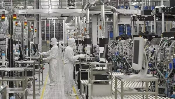
Integrated circuits are manufactured in scrupulously clean conditions; workers have to wear “bunny suits” like this to stop them contaminating the chips they’re making.
_
Clean room:
Individual transistors are many times smaller than a virus. Just one speck of dust can cause havoc and millions of dollars of wasted effort. To mitigate this risk, chipmakers house their machines in rooms that essentially have no dust. If even the smallest speck of dust or other foreign materials ends up on the wafer, it can ruin the microchip, so chipmakers are careful to keep their fabs clean. Just how clean? About 10,000 times cleaner than the outside air. Most chipmakers have ‘ISO class 1’ cleanrooms that are ‘zero dust’, meaning there are no more than 10 particles between 100 and 200 nm in size per cubic meter of air, and none larger than 200 nm. In comparison, a clean, modern hospital has about 10,000 dust particles per cubic meter. The air inside a cleanroom is filtered and recirculated continuously, and employees wear special clothing (sometimes called ‘bunny suits’) to help keep the air particle free. To maintain that environment, the air is constantly filtered and very few people are allowed in. If more than one or two workers appear on a chip production line—wrapped head-to-toe in protective equipment—that could be a sign something’s wrong. The real geniuses behind semiconductor design and development work miles away. Even with all those precautions, the wafers of silicon can’t be touched by humans or exposed to the air. They travel between machines in cartridges carried by robots that run on tracks in the ceiling. They only emerge from the safety of those cartridges when they’re inside the machines and it’s time for a key step in the process.
_______
Semiconductor device fabrication is the process used to manufacture semiconductor devices, typically the metal–oxide–semiconductor (MOS) devices used in the integrated circuit (IC) chips such as modern computer processors, microcontrollers, and memory chips such as NAND flash and DRAM that are present in everyday electrical and electronic devices. It is a multiple-step sequence of photolithographic and chemical processing steps (such as surface passivation, thermal oxidation, planar diffusion and junction isolation) during which electronic circuits are gradually created on a wafer made of pure semiconducting material. Silicon is almost always used, but various compound semiconductors are used for specialized applications.
The entire manufacturing process takes time, from start to packaged chips ready for shipment, at least six to eight weeks (tape-out only, not including the circuit design) and is performed in highly specialized semiconductor fabrication plants, also called foundries or fabs. All fabrication takes place inside a clean room, which is the central part of a fab. In more advanced semiconductor devices, such as modern 14/10/7 nm nodes, fabrication can take up to 15 weeks, with 11–13 weeks being the industry average. Production in advanced fabrication facilities is completely automated and carried out in a hermetically sealed nitrogen environment to improve yield (the percent of microchips that function correctly in a wafer), with automated material handling systems taking care of the transport of wafers from machine to machine. Wafers are transported inside FOUPs, special sealed plastic boxes. All machinery and FOUPs contain an internal nitrogen atmosphere. The air inside the machinery and FOUPs is usually kept cleaner than the surrounding air in the cleanroom. This internal atmosphere is known as a mini-environment. Fabrication plants need large amounts of liquid nitrogen to maintain the atmosphere inside production machinery and FOUPs, which is constantly purged with nitrogen.
________
For about 50 years, the number of electronic components that could be put on an individual microchip at a certain cost has doubled every few years. This trend has been described as Moore’s Law since 1965, when U.S. engineer Gordon Moore (1929–) identified it. During those decades, engineers and physicists have continually striven to make electronic components smaller so that more could be fit on each microchip. (Simply making chips larger to fit more components on them would not have worked, since the time needed for signals to travel across a sprawling chip would slow its operation.) Since the early 1990s, however, designers have been warning that miniaturization is becoming steadily more difficult as the dimensions of transistors and other integrated devices approach the atomic scale, where quantum uncertainty will inevitably render traditional electronic designs unreliable. In 2005, an industry review of semiconductor technology found that the limits of the silicon-based microchip may be reached by about 2020. They agreed that alternative technologies, such as quantum computing or biology-based approaches, all have flaws, and that there is not yet any clear successor to pick up in 2020 where silicon leaves off. But silicon is still there in 2022.
_
Manufacture of a microchip begins with the growth in a factory of a pure, single crystal of silicon or other semiconducting element. A semiconductor is a substance whose resistance to electrical current is between that of a conductive metal and that of an insulating material such as glass. This large, cylindrical crystal is then sawed into disc-shaped wafers 4–12 inches (10–30 cm) across and only 0.025–0.077 cm thick. One side of each wafer is polished and then processed to produce upon it dozens of identical microchips. These are separated after the wafer is processed, placed in tiny protective boxes called packages, and connected electrically to the outside world by metal pins protruding from the packages. In the early 2000s, manufacturers began packing multiple microprocessors onto each chip so that the processors could work in parallel, speeding computation. In 2006, the first chips to contain over 1 billion transistors appeared; in 2008, the number jumped to 2 billion. This was about 50,000 times the number of transistors in the earliest microprocessors of the 1970s.
__
To produce a microchip requires massive factories that cost billions of dollars and must be retooled every few years as technology advances. The basics of the microchip fabrication process, however, have remained the same for decades—by bombarding the surface of the silicon wafer with atoms of various elements, impurities termed dopants can be introduced into the wafer’s crystalline structure. These atoms have different properties from the silicon atoms around them and so populate the crystal either with extra electrons or with “holes,” gaps in the crystal’s electron structure that behave almost like positively-charged electrons.
Microscopically precise patterns of p-type (positively-doped, hole-rich) silicon and n-type (negatively-doped, electron-rich) silicon are projected optically onto a light-sensitive chemical coating on the wafer (a photo-resist). Because wafers are usually quite large, the process of shining light (called photolithography) through the mask must be repeated many times – often fitting hundreds or thousands of them on a single wafer. Each one will later become one single chip – a die. Other chemicals etch away the parts of the photo-resist that have been exposed to the light, leaving a minutely patterned layer. The surface of the wafer is then bombarded by dopants, which only enter the crystal where it is not protected by the photoresist. Metal wires and new layers of doped silicon can be added by similar processes. Dozens of photoresist, etching, and deposition stages are used to build up the three-dimensional structure of a modern microchip. ICs are made of layers. Each layer is only 0.005mm thick. The process can take as many as 30 to 100 layers. By crafting appropriately shaped p-type and n-type regions of crystal and covering them with multiple, interleaved layers of SiO2, polycrystalline silicon (silicon comprised of small, jumbled crystals), and metal strips to conduct current from one place to another, a microchip can be endowed with millions or billions of interconnected, microscopic transistors. Eventually tests are carried out to ensure the circuit on the die performs as desired. Due to the complexity and numerous processing steps, there are always failing dies due to manufacturing problems, even though this process is carried out in sterile environments with heavily automated equipment. Nonetheless, the good dies are identified, packaged, processed and sent all around the world.
______
______
Synopsis of chip making:
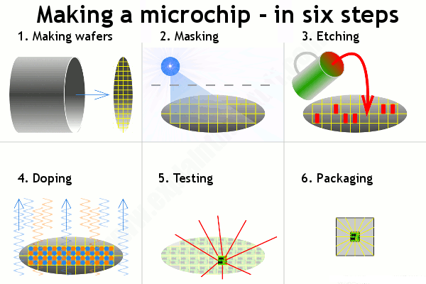
Although making a chip is very intricate and complex, there are really only six separate steps (some of them are repeated more than once). Figure above shows six key steps in making a silicon microchip: making a wafer, masking, etching, doping, testing, and packaging as seen in the figure above.
Making wafers: Pure silicon is grown into crystals of long cylinders and sliced them into thin wafers, each of which will ultimately be cut up into many chips.
Masking: Circuit building starts out by adhering a layer of silicon dioxide insulation on the wafer’s surface. The insulation is coated with film and exposed to light through the first photomask, hardening or softening the film. Photoresist is an essential material for chip creation that’s light-sensitive. Once the wafer is coated, a machine shines a UV light mask on it, which outlines the circuits’ pattern. Chips are made through a process called lithography. It’s actually very similar to photography. The only main difference is that in photography, light is used to transfer images onto film. For chips, light is used to transfer images onto a silicon surface. A wafer of silicon is meticulously patterned with an array of transistors. This process involves laying down a layer of photoresist on top of an exposed wafer and then blasting it with light to harden or soften parts of it.
Etching: The soft areas are etched away exposing the silicon base below. The soft portions must be dissolved away, typically by soaking in acid or some other chemical solvent. A chemical is used to remove some of the photoresist, making a kind of template pattern showing where engineers want areas of n-type and p-type silicon. At each stage in the circuit patterning process, another layer of photoresist is added on top and etched away until all that’s left is your final circuit design.
Doping: The etched wafers are heated with gases containing impurities to make the areas of n-type and p-type silicon. More masking and etching may follow.
Testing: Long metal connection leads run from a computer-controlled testing machine to the terminals on each chip. Any chips that don’t work are marked and rejected.
Packaging: All the chips that work OK are cut out of the wafer and packaged into protective lumps of plastic, ready for use in computers and other electronic equipment.
______
______
Wafer making:
The process of making an integrated circuit starts off with a big single crystal of silicon, shaped like a long solid pipe, which is “salami sliced” into thin discs (about the dimensions of a compact disc) called wafers. The wafers are marked out into many identical square or rectangular areas, each of which will make up a single silicon chip (sometimes called a microchip). Thousands, millions, or billions of components are then created on each chip by doping different areas of the surface to turn them into n-type or p-type silicon.
Fewer people know, all semiconductor processes start with a grain of sand. Because the silicon contained in sand is the raw material needed to produce wafers. A wafer is a round slice formed by cutting a single crystal column made of silicon (Si) or gallium arsenide (GaAs). To extract high-purity silicon materials, silica sand is required, a special material with a silicon dioxide content of up to 95%, which is also the main raw material for making wafers. Wafer processing is the process of making and obtaining wafers.
It took decades to perfect the process of producing silicon with a perfect monocrystalline structure. That begin with melting in a furnace raw polysilicon. The poly is heated to over 1,371 degrees Celsius to purge the silicon of impurities. The liquified silicon is then spun in one direction, while a silicon seed, about the size of a pen, is sent down into the molten silicon and spun in the opposite direction. Why two directions? It saves wear and tear on the expensive equipment. The silicon doesn’t care which way it is spun. So, spinning in a crucible bi-directionally speeds the ingot creation with less burden to the system. Once cooled the silicon crystal seed is pulled from the crucible at a very slow rate of about 90mm per hour. The silicon crystal weight depends on the diameter of the ingot. For example, a 200mm silicon crystal ingot is about 440 pounds. Technicians then test the purity and molecular orientation. Its then sent to diamond wire sawing. The equipment looks a giant bread-slicer. Thin wires cut the ingot into silicon wafers as seen in the figure below.
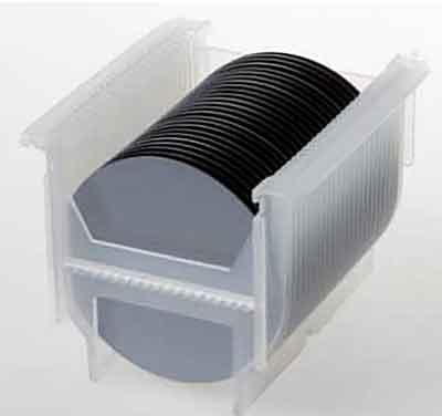
The waste created by the wire saw is called Kerf. Currently some firms are working on creating silicon by simply pouring the molten Si liquid into molds. Kerfless silicon would save greatly on expense as no amount of silicon is wasted! Solar cell manufacturing firm 1366, Inc. is at the forefront of this research. Several more procedures are then used to smooth the silicon surface to a flatness that can be used in Integrated Circuits (IC).
_
Pure silicon or poly silicon is obtained by the following steps:
-Quartz is made to react with coke to produce metallurgical silicon in an electric furnace.
-The metallurgical silicon is then converted to trichlorosilane (TCS) in fluidized bed reactors.
-Subsequently, TCS is purified by distillation, and then decomposed onto hot silicon filaments in a reactor, along with hydrogen. Finally, the resultant is a poly-silicon rod.
-The poly-silicon rod is then crystallized using Czochralski method to obtain silicon crystals or ingots. Semiconductor grade polycrystalline silicon is converted to single-crystal silicon – meaning that the randomly associated crystallites of silicon in polycrystalline silicon are converted to a large single crystal. Single-crystal silicon is used to manufacture most Si-based microelectronic devices. Single-crystal silicon ingots are finally cut into wafers using diamond wire as cutting tool.
A typical wafer (figure below) is made out of extremely pure silicon that is grown into mono-crystalline cylindrical ingots (boules) up to 300 mm (slightly less than 12 inches) in diameter using the Czochralski process. These ingots are then sliced into wafers about 0.75 mm thick and polished to obtain a very regular and flat surface.
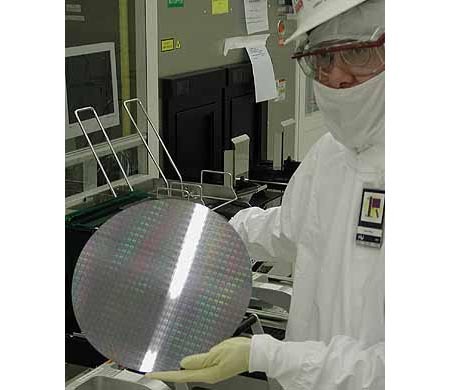
The thin slice obtained through the above-mentioned cutting process is called a “die”, that is, an unprocessed “raw wafer”. The die surface is uneven, and it is impossible to directly print circuit patterns on it. Therefore, it is necessary to first remove surface defects through grinding and chemical etching processes, then form a smooth surface through polishing and then cleaning residual contaminants.
The silicon wafers forming the base of the semiconductor are cleaned. Even slight contamination of a wafer will cause defects in the circuit. Therefore, chemical agents are used to remove all contamination, from ultra-fine particles to minute amounts of organic or metallic residues generated in the production process, or unwanted natural oxide layers generated due to exposure to air.
Then through multiple stages of masking, etching, and diffusion, the sublayers on the chip are created. The final stage lays the top metal layer (usually aluminum), which interconnects the transistors to each other and to the outside world. Most of the transistors in every chip on the wafer are created at the same time. A 300mm wafer can hold hundreds of dies (chips), which means billions and trillions of transistors are fabricated simultaneously.
_
The picture below shows an example of a silicon wafer with several individual silicon chips. How many microchips can be made from a 300mm wafer? It depends on the chip size. Below is a picture of 300 mm wafer with 16 mm x 16 mm integrated circuits (chips). You can see that there are 263 chips of them.
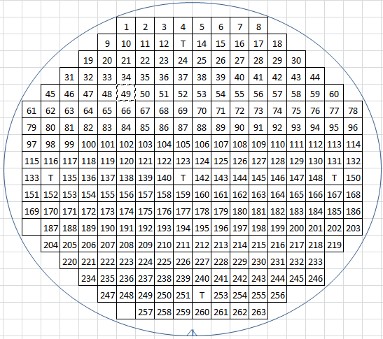
If the integrated circuits were 8 mm x 8 mm then there would be approximately 1052 of them.
The Intel’s Itanium 2 processor was released in 2002. It contained 221 million transistors and measured 19.5 mm by 21.6 mm (421 mm²). It was fabricated in a 180 nm process. The new i9-10900K processor released in Q2’20 in 14 nm technology has 9.2 mm x 22.4 mm die size. Its area is 206 mm² and estimated number of transistors is 12 billion.
______
______
Details of chip fabrication process:
An integrated circuit is a small but sophisticated device implementing several electronic functions. It is made up of two major parts: a tiny and very fragile silicon chip (die) and a package which is intended to protect the internal silicon chip and to provide users with a practical way of handling the component. This segment describes the various “front-end” and “back-end” manufacturing processes.
The manufacturing phase of an integrated circuit can be divided into two steps. The first, wafer fabrication, is the extremely sophisticated and intricate process of manufacturing the silicon chip. The second, assembly, is the highly precise and automated process of packaging the die. Those two phases are commonly known as “Front-End” and “Back-End”. They include two test steps: wafer probing and final test.
Figure below shows Manufacturing Flow Chart of an Integrated Circuit:
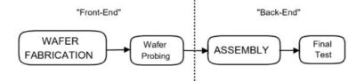
______
Wafer Fabrication (Front-End):
Identical integrated circuits, called die, are made on each wafer in a multi-step process. Each step adds a new layer to the wafer or modifies the existing one. These layers form the elements of the individual electronic circuits.
_
-1. Oxidation
The role of the oxidation process is to form a protective film of silicon dioxide (SiO2) on the surface of the wafer. It can protect the wafer from chemical impurities, prevent leakage current from entering the circuit, prevent doping during diffusion or ion implantation, and prevent the wafer from slipping off during etching.
The first step of the oxidation process is to remove impurities and pollutants, such as organic matter, metals and evaporation residual moisture with four steps. After the cleaning is completed, the wafer can be placed in a high temperature environment of 800 to 1200 degrees Celsius, and a layer of silicon dioxide is formed by the flow of oxygen or vapor on the wafer surface. Oxygen diffuses through the oxide layer and reacts with silicon to form oxide layers of different thicknesses, which can be measured after the oxidation is complete.
Dry Oxidation and Wet Oxidation Method:
According to the different oxidants in the oxidation reaction, the thermal oxidation process can be divided into dry oxidation and wet oxidation. The former uses pure oxygen to produce a silicon dioxide layer, which is slow but the oxide layer is thin and dense. The latter requires both oxygen and high solubility. The characteristic of water vapor is that the growth rate is fast, but the protective layer is relatively thick and the density is low.
In addition to the oxidizer, there are other variables that affect the thickness of the silicon dioxide layer. First of all, the wafer structure, surface defects and internal doping concentration will affect the rate of formation of the oxide layer. In addition, the higher the pressure and temperature generated by the oxidation equipment, the faster the oxide layer will be formed. In the oxidation process, it is also necessary to use dummy wafers according to the location of the wafers in the unit to protect the wafers and reduce the difference in oxidation degree.
_
-2. Photolithography
The method of transmitting geometric forms to the base of a silicon wafer is known as photolithography. In integrated circuit manufacturing, photolithography or optical lithography is a general term used for techniques that use UV light to produce minutely patterned thin films of suitable materials over a substrate, such as a silicon wafer, to protect selected areas of it during subsequent etching, deposition, or implantation operations. Typically, ultraviolet light is used to transfer a geometric design from an optical mask to a light-sensitive chemical (photoresist) coated on the substrate. The light’s wavelength plays an important role in the etching processes used to make silicon transistors. The shorter the distances between the waves, the more energetic the light and the more precise and finer the etchings. The key to creating more powerful chip is the size of the light’s wavelength. The shorter the wavelength, the more transistors can be etched onto the silicon wafer. More transistors equals a more powerful, faster chip.
The chip wafer is put into a lithography machine and subjected to deep ultraviolet (DUV) or extreme ultraviolet (EUV) light at this step. Undesired sections of silicon framework substrate or coated film are eliminated to reveal a fundamental substance or to enable the alternative substance to be coated instead of the etched layer. The photoresist either breaks down or hardens where it is exposed to UV light as seen in the figure below. The patterned film is then created by removing the softer parts of the coating with appropriate solvents.
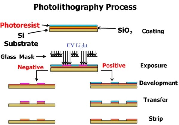
Positive Photoresists:
With positive photoresists, UV light strategically hits the material in the areas that the semiconductor supplier intends to remove. When the photoresist is exposed to the UV light, the chemical structure changes and becomes more soluble in the photoresist developer. These exposed areas are then washed away with the photoresist developer solvent, leaving the underlying material. The areas of the photoresist that aren’t exposed to the UV light are left insoluble to the photoresist developer. When working with positive photoresists in the semiconductor manufacturing industry, you receive an identical copy of the pattern, which is exposed as a mask on the wafer.
Negative Photoresists:
With negative resists, exposure to UV light causes the chemical structure of the photoresist to polymerize, which is just the opposite of positive photoresists. Instead of becoming more soluble, negative photoresists become extremely difficult to dissolve. As a result, the UV exposed negative resist remains on the surface while the photoresist developer solution works to remove the areas that are unexposed. This leaves a pattern that consists of an inverse pattern of the original, which is applied on the wafer.
Differences between positive and negative resist:
The following table is based on generalizations which are generally accepted in the microelectromechanical systems (MEMS) fabrication industry.
|
Characteristic |
Positive |
Negative |
|
Adhesion to silicon |
Fair |
Excellent |
|
Relative cost |
More expensive |
Less expensive |
|
Developer base |
Aqueous |
Organic |
|
Solubility in the developer |
Exposed region is soluble |
Exposed region is insoluble |
|
Minimum feature |
0.5 µm |
2 µm |
|
Step coverage |
Better |
Lower |
|
Wet chemical resistance |
Fair |
Excellent |
Positive and negative resist are the two forms of resist. Lithography is an important phase since it sets the size of the transistors on a chip. Resolution is defined to be the minimum feature dimension that can be transferred with high fidelity to a resist film on a semiconductor wafer. The ability to project a clear image of a small feature onto the wafer is limited by the wavelength of the light that is used, and the ability of the reduction lens system to capture enough diffraction orders from the illuminated mask.
_
Photomask is the use of light to “print” circuit patterns onto a wafer. To create the integrated circuit design that’s on a chip, light is directed onto a mask. A mask is like a stencil of the circuit pattern. The light shines through the mask and then through a series of optical lenses that shrink the image down. This small image is then projected onto a silicon, or semiconductor, wafer. The wafer is covered with a light-sensitive, liquid plastic called photoresist. When the light passes through the mask containing the circuit pattern, the circuit can be printed on the wafer coated with a photoresist film underneath. During the exposure process, the finer the printed pattern, the more components can be accommodated in the final chip, which helps to improve production efficiency and reduce the cost of individual components. The mask is placed over the wafer, and when light shines through the mask and hits the silicon wafer, it hardens (negative resist) or softens (positive resist) the photoresist that isn’t covered by the mask. Photoresist changes the chemical properties of the wafer to become “photographic paper”. The thinner the photoresist layer on the surface of the wafer, the more uniform the coating, and the finer the patterns that can be printed. The step after light exposure is to spray developer on the wafer, in order to remove photoresist in the area not covered by the mask (positive development), so that the printed circuit pattern can be revealed. After the development is completed, it needs to be checked by various measuring equipment and optical microscopes to ensure the quality of the drawing of the circuit diagram.
Note:
Both positive and negative photoresists are still used in the semiconductor manufacturing industry today, but many semiconductor suppliers opt for positive photoresists due to their higher resolution capabilities. Positive photoresists are able to maintain their size and pattern as the photoresist developer solvent doesn’t permeate the areas that have not been exposed to the UV light. With negative resists, both the UV exposed and unexposed areas are permeated by the solvent, which can lead to pattern distortions.
While positive photoresists seem to have the advantage, negative photoresists aren’t necessarily a thing of the past. Negative resists are a great material to use for those semiconductor supplies that don’t require such high resolutions. As opposed to positive photoresists, negative resists have a faster photo speed, wider process latitude and a significantly lower operating cost. Negative photoresists also have better adhesion capabilities to certain substrate materials.
Both positive and negative photoresists have their place in the semiconductor manufacturing industry, and help to produce a range of high quality products.
_
Microchip lithography devices require three fundamental techniques, and their performance is determined by them.
The first innovation is “the projection lens’s resolution capabilities.” The more complicated a circuit design that can be optically conveyed, the higher the resolution capability of the lens.
“Alignment accuracy” is the second technique. Photomasks must be changed tens of times and circuit designs must be carved continuously during the exposure process to manufacture a single transistor. As a result, the silicon wafer and photomask must be always perfectly coordinated.
The third critical factor is “throughput.” When transistors are mass-produced, this technology is critical. Throughput is a measure of efficiency that is stated as the number of silicon wafers exposed per hour.
_
Photolithography processes can be classified according to the type of light used, such as deep ultraviolet (DUV) lithography and extreme ultraviolet (EUV) lithography.
DUV: Deep ultraviolet, a wavelength range between 248 and 193 nanometres.
EUV: Extreme ultraviolet, the wavelength range between roughly 100 and 10 nanometres.
The wavelength of light used determines the minimum feature size that it can impress on the photoresist. As of 2001, deep-ultraviolet lithography used a wavelength of 240 nanometers. A nanometer is one-billionth of a meter. As chipmakers reduce to 100-nanometer wavelengths, they will need a new chipmaking technology. The problem posed by using deep-ultraviolet lithography is that as the light’s wavelengths get smaller, the light gets absorbed by the glass lenses that are intended to focus it. The result is that the light doesn’t make it to the silicon, so no circuit pattern is created on the wafer. This is where EUV lithography will take over. In EUVL, glass lenses will be replaced by mirrors to focus light. EUV lithography will clearly make integrated circuits down to 30 nanometers. By comparison, the smallest circuit that can be created by deep-ultraviolet lithography is 100 nanometers. The light used in the latest EUVL system has a wavelength of only 13.4 nanometres. This immense reduction makes it possible to make transistors about five nanometres across. Using extreme-ultraviolet (EUV) light to carve transistors in silicon wafers will lead to faster microprocessors and memory chips with similar increases in storage capacity.
_
How EUVL works:
(1. A laser is directed at a jet of xenon gas. When the laser hits the xenon gas, it heats the gas up and creates a plasma.
(2. Once the plasma is created, electrons begin to come off of it and it radiates light at 13 nanometers, which is too short for the human eye to see.
(3. The light travels into a condenser, which gathers in the light so that it is directed onto the mask.
(4. A representation of one level of a computer chip is patterned onto a mirror by applying an absorber to some parts of the mirror but not to others. This creates the mask.
(5. The pattern on the mask is reflected onto a series of four to six curved mirrors, reducing the size of the image and focusing the image onto the silicon wafer. Each mirror bends the light slightly to form the image that will be transferred onto the wafer. This is just like how the lenses in your camera bend light to form an image on film.
The entire process relies on wavelength. If you make the wavelength short, you get a better image. This entire process has to take place in a vacuum because these wavelengths of light are so short that even air would absorb them. Additionally, EUVL uses concave and convex mirrors coated with multiple layers of molybdenum and silicon — this coating can reflect nearly 70 percent of EUV light at a wavelength of 13.4 nanometers. The other 30 percent is absorbed by the mirror. Without the coating, the light would be almost totally absorbed before reaching the wafer. The mirror surfaces have to be nearly perfect; even small defects in coatings can destroy the shape of the optics and distort the printed circuit pattern, causing problems in chip function.
_
-3. Etching
After the photolithography of the circuit diagram is completed on the wafer, an etching process is used to remove any excess oxide film and only the semiconductor circuit diagram is left. To do this, liquid, gas or plasma is used to remove the unselected parts.
There are two main etching methods, depending on the material used: wet etching that uses a specific chemical solution for chemical reaction to remove the oxide film, and dry etching that uses gas or plasma.
Wet Etching:
Wet etching that uses chemical solutions to remove oxide films has the advantages of low cost, fast etching speed, and high productivity. However, wet etching has the characteristics of isotropy, that is, its speed is the same in any direction. This will cause the mask (or sensitive film) and the etched oxide film to not be completely aligned, making it difficult to process very fine circuit diagrams.
Dry Etching:
Dry etching can be divided into three different types:
The first is chemical etching, which uses etching gas (mainly hydrogen fluoride). Like wet etching, this method is also isotropic, which means that it is not suitable for fine etching.
The second method is physical sputtering, that is, ions in the plasma are used to strike and remove the excess oxide layer. As an anisotropic etching method, it has different etching speeds in the horizontal and vertical directions, so its fineness must exceed that of chemical etching. However, the disadvantage of this method is that the etching speed is slow, because it completely relies on the physical reaction caused by ion collision.
The third method is reactive ion etching (RIE). It combines the first two methods, that is, while using plasma for ionized physical etching, and chemical etching is performed with free radicals generated after plasma activation. In addition to the etching speed exceeding the first two methods, RIE can use the characteristics of ion anisotropy to achieve high-definition pattern etching.
Nowadays dry etching has been widely used to improve the yield of fine semiconductor circuits. Maintaining the uniformity of full-wafer etching and increasing the etching speed are crucial. Today’s most advanced dry etching equipment is supporting the production of the most advanced logic and memory chips with higher performance.
_
-4. Doping silicon (diffusion and ion implantation)
Diffusion is the oldest technique used to add impurity into the Substrate. The main aim of the Diffusion Process in IC Fabrication is to change the Conductivity of silicon substrate over a depth. The Diffusion Process in IC Fabrication is used in bipolar device technology to form bases, emitters, collectors; while in MOS device technology to form source and drain region. Diffusion is the process by which specific types of “impurity” atoms can be introduced into the silicon material. This doping process changes the conductivity type of the silicon so that p-n junctions can be formed. (The p-n junction is a basic building block of semiconductor devices.) Silicon wafers are oxidized to firm layer of silicon dioxide and windows are opened in thc oxide in selected areas using photolithography and etching as just described above. Dopants (or doping atoms) are purposely inserted in the silicon lattice, hence changing the features of the material in predefined areas: they are divided into “N” and “P” categories representing the negative and positive carriers they hold. Many different dopants are used to achieve these desired features: Phosphorous, Arsenic (N type) and Boron (P type) are the most frequently used ones.
There are two ways to dope the silicon. The first one is to insert the wafer into a furnace. Doping gases are then introduced which impregnate the silicon surface. This is one part of the manufacturing process called diffusion (the other part being the oxide growth).
The second way to dope the silicon is called ionic implantation. A fabrication process that is an alternative to high-temperature diffusion is ion implantation. A beam of dopant ions is accelerated to a high energy and is directed at the surface of a semiconductor. As the ions enter the silicon, they collide with silicon atoms and lose energy and finally come to rest at some depth within the crystal. Since the collision process is statistical in nature, there is a distribution in the depth of penetration of the dopant ions. Two advantages of the ion implantation process compared to diffusion are (1) the ion implantation process is a low temperature process and (2) very well defined doping layers can be achieved. Layers of oxide can be used to block the penetration of dopant atoms so that ion implantation can occur in very selected regions of the silicon.
One disadvantage of ion implantation is that the silicon crystal is damaged by the penetrating dopant atoms because of collisions between the incident dopant atoms and the host silicon atoms. However, most of the damage can he removed by thermal annealing the silicon at an elevated temperature. The thermal annealing temperature, however, is normally much less that the diffusion process temperature. Unlike diffusion, ionic implantation allows to put atoms at a given depth inside the silicon and basically allows a better control of all the main parameters during the process. Ionic implantation process is simpler than diffusion process but more costly (ionic implanters are very expensive machines). A big difference between ion implantation and sputtering is that for ion implantation there is no plasma between the substrate and the target.
Figure below shows Diffusion and Ionic Implantation Processes:
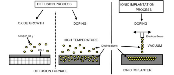
_
The processes to follow are Metallization, Bonding, and Packaging after the semiconductor devices have been fabricated. They need to be connected to each other to form the circuit. Metal films are generally deposited by a vapor deposition technique and the actual interconnect lines are formed using photolithography and etching. In general, a protective layer of silicon nitride is finally deposited over the entire chip.
_
-5. Metal Film Deposition
The conducting regions of the microchip are formed by depositing conductive metal onto the wafer. Thin film layers of silicon oxide, aluminum and other metals that will become the circuit materials are formed on the wafer. There are a variety of ways to form these thin films. To form a multi-layer semiconductor structure, we need to fabricate a device stack first, that is, alternately stacking multiple thin metal (conductive) films and dielectric (insulating) films on the surface of the wafer, and then repeat the etching process to remove excess parts and form a three-dimensional structure. Technologies that can be used in the deposition process include chemical vapor deposition (CVD), atomic layer deposition (ALD) and physical vapor deposition (PVD). The methods using these technologies can be divided into dry and wet deposition.
-A) Chemical Vapor Deposition
In chemical vapor deposition, the precursor gas chemically reacts in the reaction chamber and generates a thin film attached to the surface of the wafer and by-products that are drawn out of the chamber.
Plasma-enhanced chemical vapor deposition requires the use of plasma to generate reactive gas. This method reduces the reaction temperature and is very suitable for temperature-sensitive structures. In addition, the use of plasma can also reduce the number of depositions, which can often lead to higher quality films.
-B) Atomic Layer Deposition
Atomic layer deposition forms a thin film by depositing only a few atomic layers at a time. The key to this method is to loop the independent steps in a certain order and maintain good control. Coating the precursor on the wafer surface is the first step, after which different gases are introduced to react with the precursor to form the required substances on the wafer surface.
-C) Physical Vapor Deposition
Physical vapor deposition refers to the formation of thin films by physical means. Sputtering is a physical vapor deposition method. Its principle is that atoms of the target material are sputtered out by the bombardment of argon plasma and deposited on the wafer surface to form a thin film.
In some cases, the deposited film can be treated and improved by techniques such as ultraviolet heat treatment.
Through wafer-based lithography, etching, diffusion and deposition processes, transistors and other components can be constructed, but they also need to be connected to achieve power and signal transmission and reception.
_
-6. Interconnection:
Metal is used for circuit interconnection because of its conductivity, which is need to meet the following conditions:
-Low Resistance: Since the metal circuit needs to pass current, the metal in it should have low resistance.
-Thermochemical stability: The properties of the metal material must remain unchanged during the metal interconnection process.
-High Reliability: With the development of integrated circuit technology, even a small amount of metal interconnect materials must have sufficient durability.
-Manufacturing Cost: Even if the previous three conditions have been met, high cost is not suitable for the mass production.
The interconnection process mainly uses two substances, aluminum (Al) and copper (Co).
Aluminum Interconnection Process:
This process starts with aluminum deposition, photoresist application, and exposure and development, removing any excess aluminum and photoresist before entering the oxidation process through etching tech. After the foregoing steps are completed, repeat them until the interconnection is completed.
With its excellent electrical conductivity, aluminum is also easy to lithography, etch, and deposit. In addition, it has a lower cost and a better adhesion to the oxide film. The disadvantage is that it is easy to corrode and has a low melting point. In addition, in order to prevent the reaction of aluminum and silicon from causing connection problems, it is also necessary to add a metal deposit to separate the aluminum from the wafer, which is called a “barrier metal.”
Aluminum circuits are formed by deposition. After the wafer enters the vacuum state, the thin film formed by aluminum particles will adhere to the wafer. This process is called “Vapour Deposition” and includes chemical vapor deposition and physical vapor deposition.
_
Copper Interconnection Process:
With the improvement of semiconductor process precision and the shrinking of device size, the connection speed and electrical characteristics of aluminum circuits are gradually unable to meet the requirements. For this reason, we need to find new conductors that satisfy the requirements of both size and cost. With its lower resistance, so it can achieve faster connection speed. What’s more, copper is more reliable because it is more resistant to electromigration than aluminum, which is the movement of metal ions that occurs when current flows through the metal.
However, copper does not easily form compounds, so it is difficult to vaporize and remove it from the wafer surface. To solve this problem, we no longer etch copper, but the dielectric materials, so that metal circuit patterns composed of trenches and via holes can be formed, and then copper is filled into the aforementioned to help interconnection, which is called “inlaid process”.
_
Photomasking, etching, ionic implantation, diffusion and metal deposition processes are repeated many times, using different materials and dopants at different temperatures in order to achieve all the operations needed to produce the requested characteristics of the silicon chip.
ICs are gradually built up on top of a wafer of silicon. The whole process takes an average of three months. A typical wafer is 300 mm in diameter (about 12″), and yields around 640 10 mm x 10 mm dies. At each step, material can be deposited or etched away. Here is a cross section of an IC showing several layers:
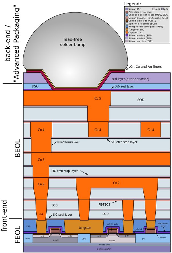
The transistors are shown at the very bottom.
The front end of line (FEOL) is the first portion of IC fabrication where the individual devices (transistors, capacitors, resistors, etc.) are patterned in the semiconductor.
The back end of line (BEOL) is the second portion of IC fabrication where the individual devices get interconnected with wiring on the wafer, the metalization layer. Common metals are copper and aluminum.
Each layer is defined by a photomask. The process is similar to how traces are laid down on a PCB.
In this example, the top layer is connected to solder balls, which are exposed on the bottom of the IC and are soldered to a corresponding pattern on the PCB. In less dense packages, wires (typically gold) connect the IC to pins on the outside of the package.
_
-7. Backlap is the final step of wafer fabrication. The wafer thickness is reduced from 650 microns to a minimum of 180 microns (for smartcard products).
All these processes are part of the manufacturing phase of the chip itself. Silicon chips are grouped on a silicon wafer (in the same way postage stamps are printed on a single sheet of paper) before being separated from each other at the beginning of the assembly phase.
_
-8. Wafer Probing:
This step takes place between wafer fabrication and assembly. It verifies the functionality of the device performing thousands of electrical tests, by means of special microprobes.
Wafer probing is composed of two different tests:
-A) Process parametric test: this test is performed on some test samples and checks the wafer fabrication process itself.
-B) Full wafer probing test: this test verifies the functionality of the finished product and is performed on all the dies.
The bad die are automatically marked with a black dot so they can be separated from the good die after the wafer is cut. A record of what went wrong with the non-working die is closely examined by failure analysis engineers to determine where the problem occurred so that it may be corrected. The percentage of good die on an individual wafer is called its yield.
_
Laser Marking:
There are two main reasons why the laser marking process is important: traceability and readability.
Traceability:
The main reason wafers are marked, so they are easily tracked throughout the manufacturing process. Semiconductors go through many steps before they are finally ready to be distributed. This includes polishing, cleaning, and testing. During this progression, it’s important to differentiate between the different wafers so that each one undergoes the necessary procedures and those that don’t meet the standards can be separated.
Readability:
Different semiconductors have different applications. Laser marking is a useful way of denoting which item is suitable for different uses. Lasers not only cut into the surface of a wafer, but they can also re-arrange the surface particles, creating marks that are minutely shallow yet easily readable.
_
Electron microscopy:
Currently, semiconductor devices are manufactured in a technology node of several nanometers. Electron microscopy is mainly used in semiconductor inspection in manufacturing stages since accelerated electrons have wavelengths of nanometers or less, and a high spatial resolution can be expected. Among various electron microscopes since the scanning electron microscope (SEM) can observe the sample as it is without processing the sample, the SEM-based inspection instrument is mainly used at each stage of manufacturing the semiconductor device.
_________
Assembly (Back-end):
The first step of assembly is to separate the silicon chips: this step is called die cutting.
Then, the die are placed on a lead frame: the “leads” are the chip legs which will be soldered or placed in a socket on a printed circuit board. On a surface smaller than a baby’s fingernail we now have thousands (or millions) of electronic components, all of them interconnected and capable of implementing a subset of a complex electronic function. At this stage the device is completely functional, but it would be impossible to use it without some sort of supporting system. Any scratch would alter its behaviour (or impact its reliability), any shock would cause failure. Therefore, the die must be put into a ceramic or plastic package to be protected from the external world. A number of operations have to be made to realize this: they are described in the figure below.
Description of the Assembly Process:
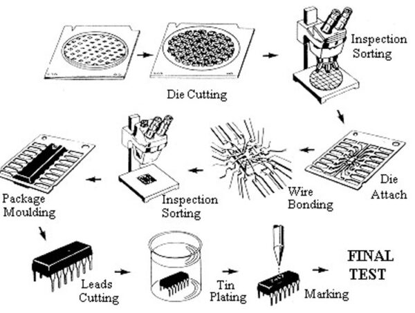
Wires thinner than a human hair (for microcontrollers the typical value is 33 microns) are required to connect chips to the external world and enable electronic signals to be fed through the chip. The process of connecting these thin wires from the chip’s bond pads to the package lead is called wire bonding.
The chip is then mounted in a ceramic or plastic package. The package not only protects the chip from external shocks, but also makes the whole device easier to handle. These packages come in a variety of shapes and sizes depending on the die itself and the application in which it will be used as seen in the figure below.
Different Kinds of Plastic Packages:
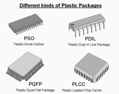
Products are then marked with a “traceability code” which is used by the manufacturer and the user to identify the function of the device (and its date of fabrication). At the end of the assembly process, the integrated circuit is tested by automated test equipment. Only the integrated circuits that passed the tests will be packed and shipped to their final destination. The chip that has the final form must pass the final defect test. All that enters the final test is the finished semiconductor chip. They will be put into the test equipment, set different conditions such as voltage, temperature and humidity, etc. for electrical, functional and speed tests. The results of these tests can be used to find defects, improve product quality and production efficiency.
______
Wafer to chip to package:
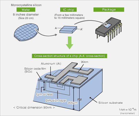
______
Yield:
Each silicon wafer contains potentially hundreds of chips, but not every chip from a wafer behaves the same. After the initial manufacturing process, each wafer gets cut into individual chips. These chips are then tested to determine how good each is in a process called binning. Some may work perfectly, others may be effectively useless (too many bad spots), while many will fall somewhere in between those extremes.
The percentage of functioning chips is the yield. Most companies won’t directly report their chip yield, though rumors and estimates suggest that Intel’s first generation 10nm process had yields in the single digits. In other words, less than 10 percent of the potential 10nm processors were viable—and that’s after Intel disabled the Gen10 graphics, and with a small dual-core die! In contrast, it’s estimated that with the harvesting of partially functioning dies, yields for AMD’s new Zen 2 parts may be 85 percent or higher.
This is important because each wafer that’s produced has a relatively fixed cost—perhaps $7,000-$10,000 or more. This is also why traditionally smaller chips are preferable to larger chips, since more chips can fit within the space of a wafer. A small 74mm^2 chip like Zen 2 has a potential of nearly 800 chips per wafer, while Intel’s 10-core Skylake-X chips are around 322mm^2 and only fit about 170 chips per wafer. With a defect density of 0.1 per cm^2, the 10-core Skylake-X might lose up to a third of the potential chips (without harvesting), while the Zen 2 CCD would only have about 8 percent defective chips.
Binning is a process through which manufacturers of chips categorize them according to their build quality and performance. Binning addresses multiple aspects of the chip. First there’s the harvesting of partially functioning dies. Binning also determines the ideal voltage and frequency, and sometimes a chip that is otherwise fully functional might get downgraded simply because it can’t run at the desired speed.
In short, the best chips get sold as the fastest, most expensive parts. Meanwhile, the functional but perhaps not quite as good chips are sold as lower tier parts. Depending on how intensive and accurate the binning process is, the gap between the ‘best’ and ‘worst’ functional chips from a wafer may be relatively small. An established process node like TSMC’s 12/16nm or Intel’s 14nm++ generally gets very good yields and relatively similar performing parts. Newer manufacturing nodes like TSMC’s 7nm or Intel’s upcoming 10nm meanwhile generally have a larger gap between ‘good’ and ‘mediocre’ parts.
______
Silicon labeling and graffiti:
To allow identification during production most silicon chips will have a serial number in one corner. It is also common to add the manufacturer’s logo. Ever since ICs were created, some chip designers have used the silicon surface area for surreptitious, non-functional images or words. These are sometimes referred to as chip art, silicon art, silicon graffiti or silicon doodling. Since ICs are printed by photolithography, not constructed a component at a time, there is no additional cost to include features in otherwise unused space on the chip. Designers have used this freedom to put all sorts of artwork on the chips themselves, from designers’ simple initials to rather complex drawings. Given the small size of chips, these figures cannot be seen without a microscope.
_____
_____
Role of plasma in chip fabrication:
None of the chips could be manufactured without using plasma. That’s because plasma technology is capable of forming transistors and wires that are much smaller than the width of a single hair. Without plasma, the transistors would have to be made much bigger, making the chips more expensive, slower, and much less powerful. Many people are not aware of significance of using plasmas to make chips for electronics.
Plasma can be created by taking an ordinary gas — like air — and adding energy until electrons are stripped from the gas atoms and molecules. Usually plasma is formed by using electricity to strip electrons from these gas particles. Those electrons become very hot typically more than 20,000ºF! The hot electrons collide with gas particles, breaking many of them apart and knocking off electrons to create electrically-charged particles called ions. One of the most common plasmas is within the fluorescent light. When the light is off, that tube is filled with argon gas and mercury, but turn on the power, and the gas inside the tube is converted to glowing plasma! Plasma is used to make computer chips.
_
Before learning how plasma is used, it’s helpful to simplify how chips are made.
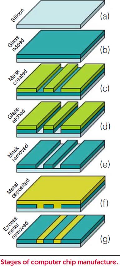
Figure above shows stages of computer chip manufacture.
Chips are made like a layer cake, but with the unwanted parts of each layer removed before the next layer is applied. To create a complex, three-dimensional chip structure layer-by-layer, the two basic steps of adding a thin layer of material and then removing its unwanted parts are repeated many times. To begin, we use a flat piece of silicon (Figure (a)). A thin layer of glass (SiO2) is added to the entire wafer as shown in (b). Next, a layer of light-sensitive film (“photoresist”) is applied to the wafer. Laser light is used to remove parts of the film. The remaining film is called a “mask”(c). It protects parts of the wafer’s surface from being removed during the “etch” step (d), where plasma process is used. Once the etching is complete, the mask is stripped away (e). Dopants are deposited on silicon. Next, a thin film of metal is deposited on top of the wafer (f). Finally, the extra metal is polished from the wafer, leaving a layer of metal wires and glass insulation (g). More glass is added to coat the top of that layer, and the entire process is repeated over and over, creating an intricate three-dimensional network of circuit wiring. Connections between layers are made by etching small holes in the glass and filling the holes with metal.
So chips are made by depositing thin layers of glass (SiO2), dopants and metal, then removing the parts of each layer that are not needed for the final chip. But how is plasma used in this process? Some of the ions and fragments of molecules in the plasma are eager to react chemically with the wafer surface. These reactive components of plasma are what make it possible for engineers to create the intricate layers of a chip.
As an example, let’s look at etching silicon (Si) using plasma.
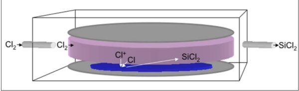
Figure above shows schematic of a silicon wafer (blue) in a vacuum chamber between two metal plates (gray). The plasma is shown as purple.
A silicon wafer is placed in a vacuum chamber between two metal plates. The gas between the plates is removed by a vacuum pump and a small amount of chlorine gas (Cl2) is allowed into the vacuum chamber. The metal plates are connected to a high voltage source that turns on and off about 10 million times per second. The high voltage on the plates causes the chlorine to become electrically charged, and a glowing plasma is formed directly above the wafer. The chlorine molecules are broken apart by the plasma into chlorine atoms (Cl) and ions (Cl+). These fragments attach to the silicon atoms at the surface of the wafer and create SiCl2 gas. This gas is pumped out of the plasma, removing silicon atoms in the process. A pre-patterned photoresist mask is used to protect portions of the silicon surface from Cl atoms, preventing specific regions of the wafer from being removed, as shown in steps (c)-(d) in figure shown earlier.
The process of depositing thin films on a wafer is the opposite of etching. To deposit solid material on a wafer, the input gas must contain the atoms to be deposited. For example, silane gas (SiH4) can be used to deposit silicon using a plasma. The plasma’s electrons break SiH4 into silicon, SiHx (x can have different values to represent different molecules), and hydrogen atoms. The silicon sticks to the surface of the wafer, and the extra hydrogen is pumped from the plasma. Within a few minutes, the silicon atoms accumulate to form a solid film of material across the entire wafer. This uniform layer of silicon then needs to be patterned with photoresist and etched to form useful devices.
Thirty years ago many of these manufacturing steps used liquid chemicals or hot gases instead of plasma. For example, simple acids were used for etching. As chips have become more sophisticated, however, the size of the transistors has become extremely small. Because acids will etch not only into the wafer but also under the mask, it is impossible to use acids to etch very small circuit patterns. Plasma, on the other hand, can etch straight into the wafer because the ions are accelerated straight from the plasma to the wafer by the high voltage used to energize the plasma. Also, since plasmas create far less hazardous waste than chemical processes, plasma-based manufacturing is much less damaging to the environment.
These are only two examples of how plasmas help create electronic chips. Plasmas are also used within the lasers needed to pattern the photoresist, and they are also used to strip the photoresist from the wafer. Finally, plasmas can create “dopant” ions that modify the electrical properties of silicon, creating transistors. In fact, about half of the manufacturing steps used to make a computer chip rely on plasma. Without these vital plasma technologies, many of today’s modern conveniences could not exist.
______
______
Why are Chips so costly?
Silicon is the second most abundant element on the earth’s crust, making up about 28% of its mass. It’s the basis for most of our rocks, clay, and sand. This implies that it should be extremely cheap to make a chip.
Well.
You will need an actual design to actually make the die for the circuit/logic itself, the CAD drawing design to fit the design with a specific fab specification and requirement; and even after finishing the design you need to simulate it to make sure it will actually work. and this is where companies get estimations of how much the chip will be able to do and handle. All these add cost before even making the chip, some designs you can just buy/license them. but some you’ll need to make it from ground either by hiring engineers and designer, or by outsourcing it to a specialised company.
Yes, silicon is one of the earth’s most abundant elements, but that doesn’t automatically make chips cheap. That silicon must be refined to a purity that was not thought possible a few decades ago. These refining steps are costly. The bulk of the cost of a raw wafer (~$500) is in this process, and the capital equipment and energy used to produce it. But $500/wafer is a far cry from the $1,600 or so that a finished memory chip wafer costs, or the $5,000-odd cost of a finished high-end processor wafer. Of that cost half or more is capital depreciation on the equipment that converts the raw wafer to finished chips. The lion’s share of the capital depreciation is lithography equipment. Its cameras have lenses that are about 5-10 feet long and around a foot in diameter, and project features onto the wafer with a resolution as fine as 38 nanometers.
Another big chunk goes to the materials processing equipment, which consists of exotic tools like plasma etchers that very precisely burn things off the wafer, deposition equipment that puts atoms-thick layers of new materials onto the wafer, furnaces that are used to coax foreign atoms into the crystal structure of the silicon, and ion implanters which are like baby atom smashers.
All this equipment is extraordinarily pricey, costing millions or even tens of millions of dollars per tool. That’s why a modern wafer fabrication plant can cost as much as $10 billion to build and equip.
The odd thing is that if you were to reduce that capital depreciation by using lower-tolerance (cheaper) equipment then you would get fewer transistors on a wafer, and that would push the chip’s cost per function higher.
Then there are issues of yield and binning. And you will have to add the cost of marketing, support, warranty, retail packaging, shipping, etc. which adds more cost to the final product price…
If you have mass produced a chip, the final price might range from less than $10 for very small chips that can be made in huge quantities to up to $100’s or even $1000’s for large and custom designs which might only made in small quantities…
The dies size drives the cost more and more and it’s not to scale, as the large die brings more challenges and higher failure rates. Limited quantities drive the cost up also as you’ll have to split the development cost to smaller quantity.
Making cheaper chip is not at all simple, and (believe it or not) today’s methods are the cheapest anyone can do.
_
Cost can be reduced with Reuse:
From the most advanced process nodes to the trailing edge of design there is talk about the skyrocketing cost of developing increasingly complex SoCs. At 16/14nm it’s a combination of multi-patterning, multiple power domains and factoring in physical and proximity effects. At older nodes, it’s the shift to more sophisticated versions of the processes and new tools to work within those processes. Progress is being made on all fronts—either with tools or methodologies or platform approaches that rely heavily on reuse. While projections show it will cost as much as $300 million to develop new SoCs at the leading edge (see figure below), the real numbers are generally much lower—generally between $20 million and $50 million, providing there is plenty of reusable IP.
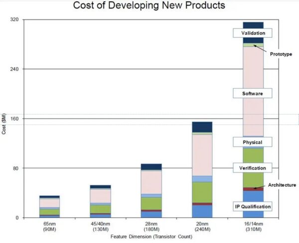
If you develop a new product from scratch it can be hugely expensive, but most folks use existing IP and software and a lot of infrastructure that comes off the tab, so it can come down to $20 million.
_______
_______
IBM created the world’s first 2nm chip in May 2021.
That sounded like a remarkable achievement, since Taiwan Semiconductor Manufacturing Company — the world’s advanced chipmaker — only started mass producing 5nm chips in 2020. IBM claims that compared to modern 7nm chips, its 2nm chips can boost performance by 45% at the same power levels, or deliver 75% more power at the same performance levels. The new 2-nanometer chips are roughly the size of a fingernail, and contain 50 billion transistors, each about the size of two DNA strands. Having more transistors will also allow more innovations related to artificial intelligence and encryption, among other things, to be added directly onto the chips. With 2-nanometer chips, cell phone batteries could last four times longer, laptops could get markedly faster and the carbon footprints of data centers could be slashed as they rely on more energy efficient chips. The 2-nanometer chips are expected to go into production starting in late 2024 or 2025, which won’t be soon enough to make a dent in the current global chip shortage.
IBM’s creation of a 2nm chip would be significant if it could mass produce and sell them on its own, or install them into its own Power systems. But IBM doesn’t manufacture its own chips anymore, it already shares its chip designs with other companies through the OpenPOWER consortium, and its most advanced 7nm Power chips are produced by Samsung — which certainly can’t mass produce 2nm chips yet. In other words, IBM’s 2nm chip is just a lab experiment. But shortly after IBM revealed is 2nm chip, TSMC fired back with a report detailing its own theoretical breakthrough with 1nm chips. However, TSMC doesn’t expect to actually hit that milestone anytime soon — it plans to mass produce 2nm chips in 2023, but anything beyond that is uncharted territory.
______
______
Chip fabrication and environmental impact:
As demand for chips surges, the semiconductor industry is trying to grapple with its huge carbon foot print. The semiconductor industry has a problem. Demand is booming for silicon chips, which are embedded in everything from smartphones and televisions to wind turbines, but it comes at a big cost: a huge carbon footprint.
The industry presents a paradox. Meeting global climate goals will, in part, rely on semiconductors. They’re integral to electric vehicles, solar arrays and wind turbines. But chip manufacturing also contributes to the climate crisis. It requires huge amounts of energy and water – a chip fabrication plant, or fab, can use millions of gallons of water a day – and creates hazardous waste.
It takes roughly 10 gallons of water to make a single computer chip. That may not sound like much, but multiply it by the millions of chips made each year, and the result is a large and rapidly growing demand for water. A typical semiconductor factory makes about 2 million integrated circuits per month and gulps about 20 million gallons of water, which ultimately must be disposed of as waste. Chips makers also use large amounts of energy and many toxic chemicals, all of which can harm the environment.
TSMC alone uses almost 5% of all Taiwan’s electricity, according to figures from Greenpeace, predicted to rise to 7.2% in 2022, and it used about 63m tons of water in 2019. The company’s water use became a controversial topic during Taiwan’s drought in 2021, the country’s worst in a half century, which pitted chipmakers against farmers.
In the US, a single fab, Intel’s 700-acre campus in Ocotillo, Arizona, produced nearly 15,000 tons of waste in the first three months of last year, about 60% of it hazardous. It also consumed 927m gallons of fresh water, enough to fill about 1,400 Olympic swimming pools, and used 561m kilowatt-hours of energy.
Chip manufacturing, rather than energy consumption or hardware use, “accounts for most of the carbon output” from electronics devices, the Harvard researcher Udit Gupta and co-authors wrote in a 2020 paper.
Making complex microchips takes a lot of chemicals and energy. A typical 2-gram silicon chip requires 1.6 kilograms of fossil fuel, 72 grams of chemicals and 32 kilograms of water to manufacture. In other words, behind those innocuous and almost weightless slivers of silicon in our ‘phones, computers and domestic appliances lies a mountain of other materials, some of which are far from friendly to the environment. The 2004 study, carried out by Eric Williams, of the United Nations University in Tokyo, and his colleagues, doesn’t imply that microchips are a bad thing. After all, the smaller the chip, the less material is needed to house it – witness the shrinking personal computer. Smarter electronic devices also use energy more efficiently. But, it suggests, efforts to make environmentally friendly chips should concentrate on reducing the energy needed to manufacture them, rather than making chips run on less power.
_
Hazardous materials in chip fabrications:
Many toxic materials are used in the fabrication process.
These include:
-poisonous elemental dopants, such as arsenic, antimony, and phosphorus.
-poisonous compounds, such as arsine, phosphine, tungsten hexafluoride and silane.
-highly reactive liquids, such as hydrogen peroxide, fuming nitric acid, sulfuric acid, and hydrofluoric acid.
It is vital that workers should not be directly exposed to these dangerous substances. The high degree of automation common in the IC fabrication industry helps to reduce the risks of exposure. Most fabrication facilities employ exhaust management systems, such as wet scrubbers, combustors, heated absorber cartridges, etc., to control the risk to workers and to the environment.
_______
_______
Section-12
Semiconductor industry:
_
Global semiconductor industry:
The semiconductor industry is the aggregate of companies engaged in the design and fabrication of semiconductors and semiconductor devices, such as transistors and integrated circuits. It formed around 1960, once the fabrication of semiconductor devices became a viable business. The industry’s annual semiconductor sales revenue has since grown to over $481 billion, as of 2018. In 2021, the sales of semiconductors reached a record $555.9 billion, up 26.2 percent with sales in China reaching $192.5 billion, according to the Semiconductor Industry Association. A record 1.15 trillion semiconductor units were shipped in the 2021.
The most widely used semiconductor device is the metal-oxide-semiconductor field-effect transistor (MOSFET), which was invented by Mohamed M. Atalla and Dawon Kahng at Bell Labs in 1959. MOSFET scaling and miniaturization has been the primary factor behind the rapid exponential growth of semiconductor technology since the 1960s. The MOSFET, which accounts for more than 99% of all transistors, is the driving force behind the semiconductor industry and the most widely manufactured device in history, with an estimated total of 13 sextillion (1.3 × 10^22) MOSFETs having been manufactured between 1960 and 2018.
The global semiconductor industry is dominated by companies from the United States, Taiwan, South Korea, Japan and Netherlands. Unique features of the industry include continuous growth but in a cyclical pattern with high volatility. While the current 20 year annual average growth of the semiconductor industry is on the order of 13%, this has been accompanied by equally above-average market volatility, which can lead to significant if not dramatic cyclical swings. This has required the need for high degrees of flexibility and innovation in order to constantly adjust to the rapid pace of change in the market as many products embedding semiconductor devices often have a very short life cycle.
At the same time, the rate of constant price-performance improvement in the semiconductor industry is staggering. As a consequence, changes in the semiconductor market not only occur extremely rapidly but also anticipate changes in industries evolving at a slower pace. The semiconductor industry is widely recognized as a key driver and technology enabler for the whole electronics value chain.
The industry is based on the foundry model, which consists of semiconductor fabrication plants (foundries) and integrated circuit design operations, each belonging to separate companies or subsidiaries. Some companies, known as integrated device manufacturers, both design and manufacture semiconductors. The foundry model has resulted in consolidation among foundries. As of 2021, only three firms are able to manufacture the most advanced semiconductors: TSMC of Taiwan, Samsung of South Korea, and Intel of the United States. Part of this is due to the high capital costs of building foundries. TSMC’s latest factory, capable of fabricating 3 nm process semiconductors and completed in 2020, cost $19.5 billion.
Intel is considering outsourcing some production to TSMC. It currently can only produce 10 nm semiconductors, while TSMC and Samsung can both produce 5 nm. GlobalFoundries, an American-headquartered firm, uses a 12 nm process for its most advanced chips due to the rapidly increasing development costs of smaller process nodes.
Chips are seen as a competitive factor between countries. While the U.S. still leads the world in chip design and intellectual property with homegrown giants like Intel Corp., Nvidia Corp. and Qualcomm, it now accounts for only 12% of the world’s chip manufacturing, down from 37% in 1990, according to Boston Consulting Group. China is the largest producer of semiconductors. It accounts for 24% of the world’s semiconductor production, followed by Taiwan at 21% and South Korea at 19%, according to the latest report from the Semiconductor Industry Association. The United States and Europe account for 10% and 8% respectively.
_
Success in the semiconductor industry depends on creating smaller, faster, and cheaper products. The benefit of being tiny is that more power can be placed on the same chip. The more transistors on a chip, the faster it can do its work. This creates fierce competition in the industry, and new technologies lower the cost of production per chip so that within a matter of months, the price of a new chip might fall 50%.
This gave rise to the observations called Moore’s Law, which states that the number of transistors in a dense integrated circuit doubles approximately every two years. The observation is named after Gordon Moore, the co-founder of Fairchild Semiconductor and Intel, who wrote a paper describing it in 1965. Nowadays, the doubling period is often quoted as 18 months—the figure cited by Intel executive David House.
As a result, there is constant pressure on chipmakers to come up with something better and even cheaper than what defined state-of-the-art only a few months before. Therefore, semiconductor companies need to maintain large research and development budgets. The semiconductor market research association IC Insights reported that the largest 10 semiconductor companies spent an average of 13.0% of sales on R&D in 2017, ranging from 5.2% to 24.0% for individual companies.
Traditionally, semiconductor companies controlled the entire production process, from design to manufacture. Yet many chip makers are now delegating more and more production to others in the industry. Foundry companies, whose sole business is manufacturing, have recently come to the fore, providing attractive outsourcing options. In addition to foundries, the ranks of increasingly specialized designers and chip testers are starting to swell. Chip companies are emerging leaner and more efficient. Chip production now resembles a gourmet restaurant kitchen, where chefs line up to add just the right spice to the mix.
In the 1980s, chip makers lived with yields (number of operational devices out of all manufactured) of 10-30%. Today, some chip makers shoot for yields of 80-90%. This requires very expensive manufacturing processes. As a result, many semiconductor companies carry out design and marketing but choose to outsource some or all of the manufacturing. Known as fabless chip makers, these companies have high growth potential because they are not burdened by the overhead associated with manufacturing, or “fabrication.”
_
The value at stake worldwide:
Many companies that need semiconductors are already reconsidering their long-term procurement strategies. Some, for instance, may shift from a “just-in-time” ordering model, which helps minimize inventory costs, to one in which they order semiconductors far in advance. For their part, many semiconductor companies are adjusting their long-standing strategies to remain strong.
The decisions that semiconductor companies make could have enormous economic significance, both for their industry and the economy as a whole. And the stakes have never been higher. In the early 2000s, profit margins were low at semiconductor companies, with most generating returns below the cost of capital. Profitability improved during the past decade, however, spurred by soaring demand for microchips in most industries, the rapid growth of the technology sector, and increased cloud usage, as well as ongoing consolidation in many sub-segments. One consequence is that the semiconductor industry’s profitability has improved significantly relative to other industries, and this trend is expected to continue.
As in any industry, value creation varies by product category, so changes in some segments could have a greater impact than others. For instance, memory has been the most profitable segment, followed by fabless companies that design their own chips but outsource their manufacture. Some regional variations are also obvious. North America, home to some of the largest fabless players, accounted for approximately 60% of the global semiconductor value pool during the 2015-19 period. Europe accounted for 4% of the industry’s total economic profit, which accrued primarily to capital-equipment companies. Asia, still the hub for contract chip manufacturing, accounted for the remaining 36%. With this geographic spread, value creation within the semiconductor industry can affect economies worldwide.
_
Next steps for a critical industry:
Capital markets have rewarded the semiconductor industry’s surging profitability, with companies in this sector delivering an annual average of 25% in total returns to shareholders from the end of 2015 to the end of 2019. In 2020, shareholders saw even higher returns, averaging 50% per annum, as consumers and businesses upped their purchases of digital equipment of all kinds, partly in response to the COVID-19 pandemic. The question is whether the semiconductor industry can continue delivering such strong returns, especially as the pandemic continues to create uncertainties about demand patterns, supply chains and other issues.
Beyond increasing production capacity, semiconductor companies could consider several steps to continue their growth and meet customer demand. They could undertake more M&A deals and partnerships to gain an edge in profitable segments and expand their customer base. Semiconductor companies might also increase investments in innovative technologies that will help them develop leading-edge chips for autonomous cars, the internet of things, artificial intelligence, and other areas with burgeoning growth. Above all, more agile strategies may be important during these uncertain times.
No matter what tactics they implement, the decisions that semiconductor companies make will reverberate far beyond their industry to touch the high-tech, consumer goods and automotive companies that depend upon them.
_______
_______
Operating Models in semiconductor industry:
Different levels of specialization and functional delineation have led to the emergence of two key operating models in the semiconductor industry: IDM, for integrated device manufacturer, and fabless-foundry.
Figure below diagrams these two models along with the industry participants, including R&D companies, and identifies some companies representing different activities in the semiconductor value chain.
In the IDM model, one company carries out all stages of production—design, manufacturing, and assembly, testing, and packaging. In the fabless-foundry model, production is split: Design companies focus on design and contract out manufacturing (fabrication), and are thus “fabless.” Foundry companies concentrate on contract manufacturing. A third group of companies, though not part of the fabless-foundry name, perform assembly, testing, and packaging. This third group is known as outsourced semiconductor assembly and test companies, or OSATs.
Operating Models in the Semiconductor Industry:
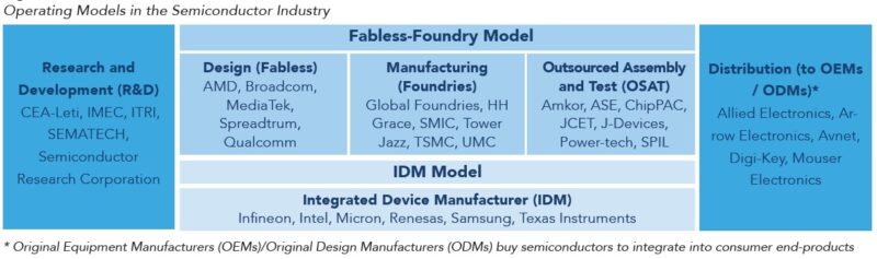
_
The IDM model derives efficiencies from vertical integration. The fabless-foundry model derives efficiencies from delineation of tasks and specialization. The fabless companies focus on design and innovation and avoid heavy investment in setting up, maintaining, and upgrading foundries. Foundries try to achieve high capacity utilization and efficiency by servicing many fabless companies in the market. OSATs focus on achieving operational efficiencies by also serving many companies to ensure a profitable capacity utilization rate, just as foundries must.
In the past decade, IDMs have been acquiring more characteristics of the fabless-foundry model. Several IDMs contract with other companies to manufacture chips while performing all other remaining tasks internally. This is commonly called fab-lite. Many IDMs become fab-lite due to the constant and costly need to upgrade manufacturing facilities to keep up with technological advances.
________
________
Semiconductor value chain:
Just like the complex and interconnected nature of a semiconductor itself, the semiconductor industry, with $555.9 billion in global sales in 2021, is distinguished by a highly specialized, globally dispersed, and interconnected value chain. This value chain and a host of supporting activities form a complex and global semiconductor ecosystem. Countries that participate in this global value chain or supporting activities reap countless benefits, including increased employment and export opportunities. The benefits compound with greater and lasting participation in that global ecosystem.
_
Semiconductor production begins with R&D and ends with distribution as seen in the figure below. After research and before distribution come design, manufacturing, and assembly, testing, and packaging. Although research and distribution are not strictly speaking production activities, they are included in the production chain because of their critical importance and their role in the value chain.
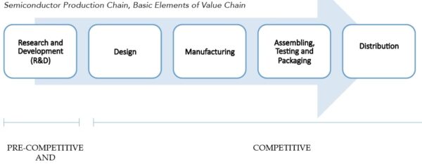
_
The ubiquity of semiconductors explains in part why the ecosystem is global. The extreme complexity of the industry provides a deeper explanation. The nonstop, consumer-driven demand for more and better capabilities, features, reliability, and speed requires a heavy investment in research and development (R&D), design, and efficient, low-cost manufacturing, testing, assembling and packaging, and distribution. These same pressures also affect the supporting activities, such as the production of semiconductor manufacturing equipment, development of design software and semiconductor intellectual property cores (“IP cores” or “IP blocks”), and provision of raw materials. These pressures have led semiconductor companies to develop business models that look beyond national borders to achieve efficiencies to compete in the marketplace.
Over the years, demands for new technology innovations that rely on chips have become even greater: Simple scaling and cost reductions based on Moore’s Law will soon no longer be enough to improve device performance. The industry is rapidly moving into new areas such as brain-inspired computing, the Internet of Things, energy-efficient sensing, automated devices, robotics, and artificial intelligence calling for new breakthroughs. A globally interdependent industry that pools the best each participant has to offer provides the best path to the future.
_
Few industries, if any, have a value chain and ecosystem so complex, geographically widespread, and intertwined. For example, one U.S. semiconductor company has over 16,000 suppliers worldwide. More than 7,300 of its suppliers are based in 46 different American states and more than 8,500 of its suppliers are located outside of the United States. Many of those suppliers are small businesses in multiple industries that provide a variety of goods and services including chemical gases, materials, construction services, foundry services, capital equipment, spares, control and life systems, computing hardware, market research, technical consulting, and media services. The industry is uniquely structured to derive maximum benefit from the diverse and varied skills of human resources and locational advantages of participating countries. Canada, European countries, and the United States tend to specialize in semiconductor design, along with high-end manufacturing. Japan, the United States, and some European countries specialize in supplying equipment and raw materials. China, Taiwan, Malaysia and other Asian countries tend to specialize in manufacturing, assembling, testing and packaging. Canada, China, Germany, India, Israel, Singapore, South Korea, the United Kingdom, and the United States are all major hubs for semiconductor R&D. Major semiconductor companies have located facilities in countries as far flung as Costa Rica, Latvia, Mexico, South Africa, and Vietnam.
This international structure evolved over decades and is still changing. In the 1950s, individual companies tended to engage in all stages of production and operated in one country. The industry is now characterized by an ever-diversifying range of business models and relationships crossing national and regional boundaries. Technological advances and competition have driven this evolution. Even companies that remain vertically integrated produce in multiple countries and not all are as integrated as in the past. For instance, for a subset of their products or technologies, they may turn to other companies for some specialized design or production. A significant number of these specialist companies operate throughout the world.
This global ecosystem benefits all participants and their global economies. Countries experience increased employment, derivative innovation, export opportunities and overall economic growth. Benefits accrue at all segments of the value chain, including those segments involving lesser investments in R&D and plant and equipment. The contribution of a country to the value of semiconductors increases as the country’s economy and the skills of its workforce grow and the country moves up the value chain. Newer countries join the value chain and start to move up. The global value chain thus expands and spreads the benefits that come with it. Companies, wherever based, benefit from productivity gains, cost efficiencies from specialization, and gains from improved technology and increased knowledge.
_
Yet, because the industry is so dynamic and a key driver of economic growth and technological innovation, a country may be tempted to create and operate a fully domestic industry by attempting to reproduce the entire value chain within its own borders. But trying to do so not only ignore the experience of several economies that have successfully participated to their benefit in the global value chain, but also risks undermining domestic industry capabilities and competitiveness. As the history of the past 50 years along with economic fundamentals demonstrate, innovation accelerates and is profitable when the industries within each country specialize in tasks they can best perform, and in which participants collaborate across the entire value chain, share knowledge, and exploit each other’s relative advantages. This is different from most other less complex industries where simply adding productive capacity or implementing protectionist measures may be enough to enable an emerging industry to be competitive.
_
The semiconductor industry is extremely complex. Products constantly improve through technological advances, production now requires numerous distinct and divergent processes, and there is constant demand for more speed, reliability, capabilities, and features. Given this complexity and the forces of competition, the semiconductor industry has evolved into an increasingly specialized and complex value chain, with different firms focusing on more specialized, activities within the production process. This delineation extends through the entire ecosystem. Participation in this worldwide ecosystem has been demonstrated to be an essential part of success for individual firms and the industry as a whole.
_
The current semiconductor ecosystem and value chain are dispersed geographically, with companies specializing in specific activities based on their inherent advantages. The result is a truly global and interdependent semiconductor value chain and ecosystem that have benefited the industry by spurring innovation and technological advancements. It has also benefited the participating countries (and firms within them) by providing competitive employment and opportunities for growth and expansion.
_
Governments can create policies that facilitate integration into global value chains. These include policies that support open to international trade (removal of tariff and non-tariff barriers), establish a transparent and predictable investment environment and ensure sound legal systems and intellectual property protection. Such steps would be far more effective than an insular strategy, which risks wasting precious resources and time, hinders the ability of semiconductor and downstream industries from moving to the next level of innovation and growth, and ultimately impedes a nation’s economic growth. The greater opportunities lie with full-fledged participation in the global value chain of one of the world’s most dynamic and vital industries.
_______
_______
A Single Company TSMC in Taiwan makes 92% of the World’s most sophisticated Chips:
Taiwan Semiconductor Manufacturing Company (TSMC) holds 53% of the Global Semiconductor Foundry market (Q2 2021). It manufactures all kinds of chips, from simple to complicated to technology bound. It is currently the company which the world is relying on for chips. TSMC manufactures chips for various companies which don’t manufacture chips but design them, such as Qualcomm Inc and Apple Inc. The chips produced by TSMC are built for various electronic devices like iPhones, cars, etc. Other companies are equally big, but they produce specific chips for specific purposes, and this is why they don’t qualify as the largest computer chips manufacturing company. TSMC holds the capacity to produce all kinds of chips, which is why companies like Apple rely on it. Almost all microchips that go into all new vehicles including Audi come from TSMC in Taiwan.
Its technology is so advanced that it now makes around 92% of the world’s most sophisticated chips, which have transistors that are less than one-thousandth the width of a human hair. Samsung Electronics Co. makes the rest. Most of the roughly 1.4 billion smartphone processors world-wide are made by TSMC.
Other countries would need to spend at least $30 billion a year for a minimum of five years “to have any reasonable chance of success” in catching up with TSMC and Samsung, wrote IC Insights, a research firm, in a recent report.
Taiwan Semiconductor Manufacturing Co Ltd is planning to build several more chipmaking factories in the U.S. state of Arizona beyond the one currently planned.
_____
_____
List of the top semiconductor companies across the world, based on their total revenue in 2020:
-1. Intel (INTC)
2020 Revenue: $77.87 billion
Total Assets: $153.09 billion
Headquartered in California’s famed Silicon Valley, Intel is a massive semiconductor company with over 110,000 employees across 46 countries. The company was founded in 1968, and since then, has grown to become the largest revenue giant among the semiconductor companies. When it comes to semiconductors, Intel is the developer of the x86 series of microprocessors, which are often found in laptops and other PCs. The company provides these microprocessors to major computer and technology companies, such as Lenovo, HP, and Dell. Intel also produces more than just semiconductors, as some of the company’s predominant products include motherboard chipsets, network interface controllers, integrated circuits, flash memory, graphics chips, embedded processors, and more. Since 2009, Intel has made over 31 worldwide acquisitions, which has landed them in the top 50 of the United States Fortune 500 list for the corporations by total revenue.
-2. Samsung Electronics
2020 Revenue: $52.2 billion
Total Assets: $304 billion
Founded in 1969, this South Korean electronics company is one of the largest producers of semiconductors in the world. Globally, the company employs almost 290,000 people and operates in 74 countries. Samsung’s semiconductors are often used in smartphones and tablets, especially in the company’s line of Samsung Galaxy devices. However, semiconductors aren’t the only product Samsung produces, as they also manufacture lithium-ion batteries, image sensors, and camera modules and displays, to name a few. For the most part, some of the company’s most prominent clients are Apple, Sony, HTC, and Nokia. Overall, Samsung is the largest manufacturer of mobile phones and smartphones, making them an extremely relevant and important company in 2021.
-3. Taiwan Semiconductor Manufacturing Co. (TSMC)
2020 Revenue: $45.5 billion
Total Assets: $89.87 billion
Taiwan Semiconductor Manufacturing Co. (TSM) is the largest manufacturer of semiconductor chips. While Intel earns more revenue, TSM makes around 90% of advanced chips produced globally. TSM also controls more than half of the global semiconductor foundry market, by revenue. As the world’s largest dedicated independent semiconductor factory, it’s no surprise that Taiwan Semiconductor Manufacturing Co. (TSMC) is one of the largest companies in Taiwan, and in the world. This company has grown rapidly since 1994, with a compound annual growth rate (CAGR) of 17.4% in revenue. Today, TSMC employs over 50,000 people and produces over 10 million semiconductor wafers per year. The most prominent devices featuring TSMC’s semiconductors are Apple products, from the MacBook Air to the iPhone 12.
-4. SK Hynix Inc
2020 Revenue: $25.27 billion
Total Assets: $56.08 billion
Specializing in the production of memory semiconductors SK Hynix Inc., formally known as Hyundai Electronics, is a South Korean company with locations in Korea, the United States, China, and Taiwan. In South Korea alone, the company employs over 22,000 people. As mentioned, SK Hynix is a major producer of memory semiconductors, or memory chips. These memory chips have several major consumers, including Apple, Asus, Dell, and HP. Additionally, the company manufactures other electronics as well, from DVD Players to cell phones.
-5. Broadcom Corporation
2020 Revenue: $23.89 billion
Total Assets: $75.93 billion
Established in 1991, Broadcom is a public American company headquartered in Irvine, California. The company’s expertise in producing semiconductors ranges from computers to smartphones, and they produce for dozens of major companies. Common clients include Apple, Motorola, IBM, Dell, Asus, Lenovo, Logitech, Nokia, and even Nintendo. Much of the interest in Broadcom’s products stems from their chip’s ability to speed up tasks that utilize encryption. For many companies, these chips aid in e-commerce and secure communications. Broadcom also produces the “BCM43″ series chips that specialize in providing WiFi support in many smartphones. Unlike other companies on this list, both Apple and Android devices utilize these chips.
-6. Qualcomm
2020 Revenue: $23.53 billion
Total Assets: $35.59 billion
Founded and Headquartered in Southern California, Qualcomm is a semiconductor company that also specializes in software and other wireless technologies. Compared to other companies on this list, Qualcomm manufactures semiconductors for a very wide range of devices, from vehicles to watches, laptops to smartphones, and WiFi. Qualcomm is known as a rather innovative company. In 2017, the company stepped out of its comfort zone to create its first PC server chip called Centriq 2400. The chip was a success, resulting in them expanding to manufacture more PC semiconductors and other electronics. Qualcomm was one of the first to manufacture 5G technology as well, with over 20 mobile devices now utilizing the company’s 5G technology.
-7. Micron Technology
2020 Revenue: $21.43 billion
Total Assets: $53.68 billion
Micron Technology is the only Idaho-based semiconductor company on this list and specializes in manufacturing memory and data storage for computers. Currently, the company employs roughly 40,000 people and maintains 18 worldwide locations. In the past two years, Micron released quite a few impressive products. In 2019, the company manufactured the first microSD card with a storage capacity of 1 terabyte (TB). In fact, as of 2020, Micron produces the largest SSD in the world: the 3.84TB Micron 5210 Ion.
-8. Applied Materials
2020 Revenue: $17.2 billion
Total Assets: $22.35 billion
Applied Materials is a Silicon Valley giant specializing in the production of semiconductors for electronics, computer displays, smartphones, televisions, and solar products. This American company was founded in 1967, and today employs over 20,000 employees. In all likelihood, this company would be higher on this list if it weren’t for a scrapped 2013 merger with Tokyo Electron, which was the largest manufacturer of semiconductor equipment at the time. Applied Materials not only specializes in manufacturing semiconductor chips but also supplies valuable equipment used to make the chips. For instance, the company’s equipment helps produce coatings for flexible electronics.
-9. Nvidia Corporation
2020 Revenue: $14.78 billion
Total Assets: $26.88 billion
Also headquartered in California’s Silicon Valley, Nvidia is a unique semiconductor company specializing in graphics processing units (GPUs), that are especially useful for computer gaming. The company’s GPU line, known as “GeForce” is the most popular graphics processor in the United States, and the Nvidia GeForce RTX 3060 Ti is currently the most powerful gaming GPU as well. While gaming is one of Nvidia’s main markets, the company’s GPUs are also used in supercomputing sites around the world. More recently, the company has also provided processors for smartphones, vehicles, and other devices.
-10. Texas Instruments Inc.
2020 Revenue: $14.46 billion
Total Assets: $19.35 billion
Texas Instruments (TI) is one of the oldest semiconductor companies on this list, being founded over 90 years ago in 1930. Today, the company has almost 30,000 employees, and mainly develops analog chips and embedded processors. TI is a rather historic semiconductor company, producing the world’s first commercial silicon transistor, (1954), integrated circuit (1958), handheld calculator (1967), and DLP chip (1987). In 2020, TI’s products are utilized in almost every electric device out there, making the company a vital indicator of the semiconductor industry’s health.
______
______
Global semiconductor sale:
Global semiconductor sale in 2020 is depicted in the figure below:
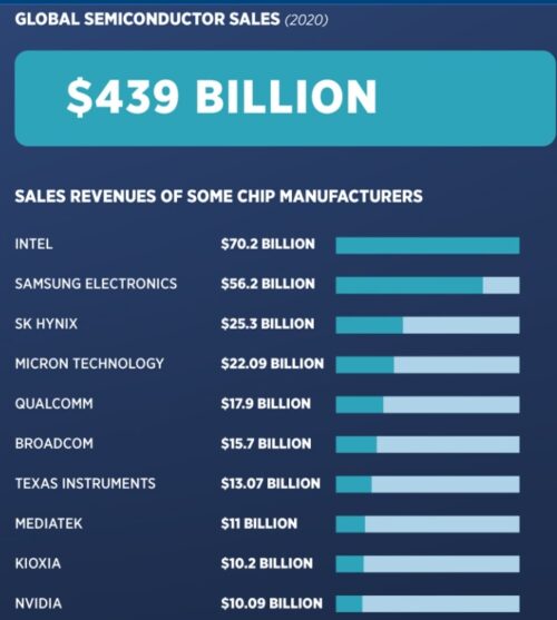
In 2021, amid the ongoing global chip shortage, semiconductor companies substantially ramped up production to unprecedented levels to address persistently high demand, resulting in record chip sales and units shipped. Demand for semiconductor production is projected to rise significantly in the years ahead, as chips become even more heavily embedded in the essential technologies of now and the future.
-In 2021, global semiconductor industry sales reached a record $555.9 billion, up 26.2% year on year.
-China remained the biggest market with sales there totalling $192.5 billion in 2021.
-The industry shipped a record 1.15 trillion semiconductor units in 2021.
______
______
Semiconductor is at the heart of US-China tech tensions:
When Singapore-based chip maker Broadcom attempted to acquire US firm Qualcomm in a more than $100 billion deal, the Trump administration vetoed the deal citing ties to Chinese firms. Besides Qualcomm, Trump cut off a planned acquisition of Oregon-based Lattice Semiconductor by a little-known private equity firm with ties to China’s government. Meanwhile, Qualcomm is on track to scrap (paywall) a planned $44 billion acquisition of Netherlands-based chip maker NXP after failing to secure approval from Chinese regulators.
Why are the world’s two most powerful nations sparring over semiconductors?
While we often hear about the internet or software companies that are wielding more and more influence over society, those companies make their breakthroughs off the advancements of chip makers. Simply put, innovation in semiconductors leads to innovative products.
Second, chips are an economic boon. The US chip industry directly employs about 250,000 people, and generates $164 billion in sales each year. When clusters of semiconductor factories are built, entire sub-industries can evolve around serving them. A manufacturing facility needs power, it needs water, it needs chemicals, it needs other raw materials, it needs equipment, it needs service. There is just a huge amount of value created around that factory.
Third, a small but critical portion of the semiconductor industry has specific applications in the defense sector, for use in things like missiles and radars. Mastery of the semiconductor technology can help ensure that a country’s military technology remains at the cutting edge.
As a result of these factors, dominance of the chip industry can give governments amazing political leverage over other countries. There’s no better example of this than when the US Department of Commerce ordered a ban on sales to ZTE. Without access to Qualcomm’s processors, the phone maker had to halt production and could have gone out of business, if not for a subsequent reprieve from the Trump administration. ZTE incident likely heightened the sense of urgency felt by policy makers in Beijing to ramp up the country’s semiconductor prowess. They need to make their own chips, so their companies can function without imported chips.
The semiconductor industry remains one of the few manufacturing-driven sectors where the US remains the global leader. After Texas Instruments’ Jack Kilby invented the integrated circuit in 1958, the US military embraced the technology as the Cold War ramped up, and consumer electronics companies later followed once the personal computer hit the market. Most of the fabrication for the country’s largest integrated circuit makers takes place within the United States. Meanwhile, the world’s most sophisticated semiconductor firms—which include Qualcomm, Nvidia, Intel, AMD, and Micron—all reside stateside.
China, meanwhile, is by far the world’s largest purchaser of semiconductors—but its share of global sales still remains marginal. According to Bernstein Research, China purchased approximately $160 billion in semiconductors in 2016, but sold only $20 billion. In other words, semiconductors are China’s biggest import by value—putting it ahead even of China’s oil imports, according to the South China Morning Post.
Why China can’t crack semiconductors?
Given China’s manufacturing prowess in general—it’s the “world’s factory,” after all—its lag in semiconductors seems surprising on the surface. Three of the world’s top-five smartphone companies are Chinese. Factories in southern China can reverse engineer hoverboards and e-cigarettes, and manufacture millions of them on the fly. Why can’t it simply dismantle Qualcomm’s chips, figure out how they’re made, and start producing them en masse?
Experts say it’s because semiconductors are some of the most complicated products to design and produce on earth.
For one thing, the R&D necessary to make advancements in chip design can span decades. There are no shortcuts to understanding the recipe of a chip. It can take an American company years just to design one chip. Then let’s say you’ve got 5,000 engineers that can reverse engineer the chip and look at the chip layout—by the time you’ve done that, the American company’s already two generations ahead of you.
Beyond designing chips, there are also barriers to manufacturing them. Setting up a fabrication facility can cost $10 billion to $15 billion. Inside those facilities are complex machines designed to carry out etchings and moldings at a microscopic level. For Intel, TSMC, Micron, and other chip manufacturers, their processes are highly proprietary, and you’re literally dealing with a process that is one atom at a time. That knowledge base is not something that you can just go and copy overnight.
Factories also need to crank out these chips quickly and consistently, with as few defects as possible. Making integrated circuits is highly complex, massive scale, and high precision. You need to produce every day, every month, to a degree where you can support say 1.5 billion smartphones every year.
Analysts say that China’s semiconductor makers remain broadly five to 10 years behind world-class companies in the US, South Korea and Taiwan. China’s manufacturers can easily make chips that power the iPhone’s fingerprint sensor—despite being a relatively new feature, the underlying technology isn’t that different from what powers a smartphone’s camera. However, producing systems-on-a-chip (SoCs) that power 4G connectivity inside high-end smartphones at scale—like those designed by Qualcomm– remains out of reach for most of China’s top semiconductor manufacturers. As a result China’s telecom sector looks set to remain hugely reliant on US chips for several years—while chip makers like Qualcomm are hugely reliant on China for their revenues.
Can money make competitive semiconductors?
China will need more than just cash to start making competitive semiconductors—it will need better engineers, managers, and bureaucrats capable of catching up in a sector that other countries have amassed decades of knowledge in.
Chip wars:
Controlling advanced chip manufacturing in the 21st century may well prove to be like controlling the oil supply in the 20th. The country that controls this manufacturing can throttle the military and economic power of others. In 2019, the US Commerce Department banned telecoms giant Huawei from buying parts and components from US companies without government approval. The Trump administration claimed Huawei endangered national security. Then in May 2020, the department added more restrictions, by issuing rules that stipulated foreign manufacturers using American-made machinery or software must obtain a special license to design or produce semiconductors for Huawei. By December 2020, the Trump administration had already blacklisted SMIC, China’s largest semiconductor foundry. The company says this will affect its R&D efforts and capacity to produce cutting-edge chips of ten nanometers (nm) and below.
China increased the purchase of Taiwanese semiconductors between 2018 and 2021 after the US sanctioned Chinese hi-tech giants Huawei and Semiconductor Manufacturing International Corporation. During the period considered, the share China’s microchip market by Taiwanese companies rose by 4.4 per cent; above all, orders for memory chips produced on the island grew by 57 per cent. China has never ruled out taking Taiwan by force. According to several experts, taking over Taiwan’s semiconductor industry is one of the goals that could lead China to attack. In fact, if chip imports from the island continue to grow, Beijing might speed up its aggression plans. However, as the Russian-Ukrainian conflict shows, a war in the Taiwan Strait risks disrupting supply chains while Chinese bombings could hit Taiwanese plants, damaging the production of irreplaceable microchips. So Washington should be worried. If the United States were to be deprived of access to Taiwanese foundries, the U.S. defense and consumer electronics industries would be set back for at least five years. Moreover, because China is investing in its own chip foundries, it could become the world leader in technology for the next decade or more. That’s why it was encouraging to see Republicans and Democrats in the House and Senate propose $250 billion to help America’s semiconductor industry.
______
______
Can United States regain edge in Chip Manufacturing?
The United States is developing new strategies to prevent it from falling further behind Korea, Taiwan, and perhaps even China in semiconductor manufacturing, as trade tensions and national security concerns continue to grow. For years, the U.S. has been a leader in the development of new chip products like GPUs and microprocessors. But from a chip manufacturing standpoint, the U.S. is losing ground in two critical areas. First, Intel and U.S. foundries are lagging in process technology against their Asian rivals in TSMC and Samsung. China is also closing the gap. Second, the U.S. has seen a sharp decline in new fabs and capacity. The U.S. isn’t behind in all manufacturing segments. But chip manufacturing is critical for maintaining technical leadership, both from a supply chain and economic perspective, as well as for security reasons.
_
For years, U.S. companies were among the leaders in developing new chip products and manufacturing them in their own wafer fabs. And until 2011, when Intel introduced the first finFETs at 22nm, they led in process technology, which is a critical ingredient for chip scaling. Each new process enables smaller and faster devices. But times have changed. Today, the dynamics are very different on the technology front, and they point to some alarming trends in the U.S. “We’ve been losing leadership in semiconductor manufacturing for a long time,” said Wally Rhines, CEO Emeritus at Mentor, a Siemens Business. “What’s even more important is leadership in the ability to provide leading-edge foundry services, which is much more than just manufacturing.” This is a complex issue with a number of different facets. On one front, for example, the U.S. lags in a former stronghold—process technology. Intel, the U.S. technology leader, recently delayed its new process, causing it to fall further behind TSMC and Samsung on this front.
_
While Intel vows it will fix the problem and get back on track, this has national security implications. Having leading-edge processes onshore is essential for the U.S. Department of Defense and military/aerospace companies, as well as for business competitiveness. “You dominate chips and you dominate the defense, technology and intelligence industries,” said Robert Maire, president of Semiconductor Advisors, in a recent presentation. “Obviously, that goes hand-in-hand with global domination. One of the reasons the U.S. is so dominant is because of our technology, and that’s grounded in the semiconductor industry.” At the same time, chipmakers continue to build new fabs in the U.S. at a slower pace than their Asian rivals.
_
The U.S share of worldwide installed wafer fab capacity has declined from 37% in 1990 to 12% in 2020, according to the U.S. Semiconductor Industry Association (SIA) and Boston Consulting Group (BCG). During the same period, Asia saw a meteoric rise in the development of new fabs to the point where it now accounts for 80% of the world’s capacity. China, in particular, has a very ambitious semiconductor agenda. Backed by $150 billion in funding, the country is developing its domestic IC industry and plans to make more of its own chips. To make matters worse, Greater China — which encompasses China, Hong Kong and Taiwan — is a geopolitical hotspot, and the U.S.-China trade war is compounding tensions in an area where all of the leading process technology is located today. Any disruption would have a major impact on U.S. access to leading-edge process technology.
_
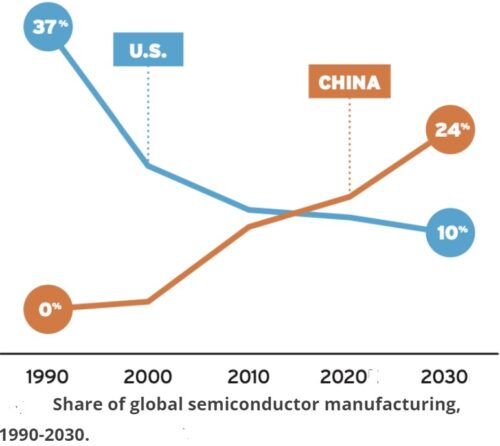
Figure above shows share of global semiconductor manufacturing, 1990-2030.
U.S. policymakers recognize the needs to build more domestic fabs, but it’s an expensive undertaking. A leading-edge fab runs from $10 billion to $20 billion, and a return on investment isn’t guaranteed. And while manufacturing is critical, it is only one piece of the competitive equation. U.S.-based companies continue to lead in chip design, specialty processes, EDA tools and fab equipment. Nevertheless, steps are being taken to shore up U.S. competitiveness on all fronts.
_
The process race:
U.S.-based chipmakers are holding their own in specialty processes like III-V, analog and RF. The U.S. is strong in mature logic processes at 28nm/22nm and above. “The U.S. continues to have a base of mature products still manufactured in the U.S.,” Semico’s Downey said. “In most electronic devices, every leading-edge chip requires at least 5-10 mature chips to go along with it. Companies such as Qorvo, ON Semi, NXP, ADI, Broadcom, Skyworks and Microchip all have fabs in the U.S. SkyWater is an example of a foundry breathing new life into an old fab by providing innovative options and helping to develop new solutions.” But the U.S. is behind in leading-edge logic/foundry processes. It wasn’t always that way. For years, Intel was the leader in process technology, but it wasn’t the only contender. In 2001, there were 18 chipmakers that could process leading-edge 130nm chips. Over time, process costs escalated and fewer players could afford to develop leading-edge technologies at advanced nodes.
_
The big change occurred at 20nm, when traditional planar transistors hit the wall. In response, Intel in 2011 moved to next-generation finFET transistors at 22nm. Foundries moved to finFETs at 16nm/14nm. (Intel’s 22nm is equivalent to 16nm/14nm from the foundries.)
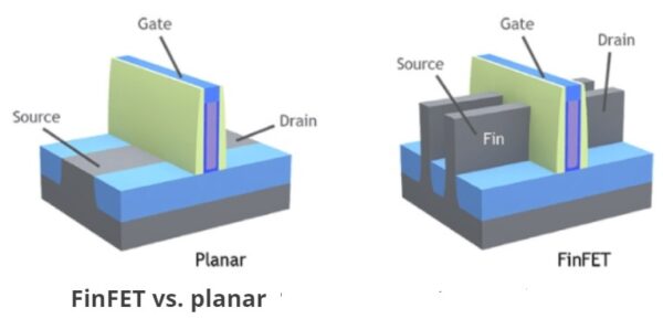
Figure above shows FinFET vs. planar.
A fin field-effect transistor (FinFET) is a type of 3D multi-gate MOSFET (metal-oxide-semiconductor field-effect transistor) built on a substrate where the gate is placed on two, three, or four sides of the channel or wrapped around the channel, forming a double or even multi gate structure. FinFETs are three-dimensional structures with vertical fins forming a drain and source. MOSFETs are planar devices with metal, oxide, and semiconductors involved in their basic structure. FinFETs have an excellent subthreshold slope and a higher voltage gain than planar MOSFETs. FinFETs provide more performance at lower power, but they are also harder and more expensive to manufacture. That’s due to the number of processing steps required to make that device. FinFETs also narrowed the manufacturing base. Only a half-dozen foundries/IDMs have the resources to migrate to finFETs at 16nm/14nm. These vendors include GlobalFoundries, Intel, Samsung, TSMC and UMC. China’s SMIC recently entered the 14nm finFET market.
_
In 2016, meanwhile, Intel hoped to extend its lead in logic technology with the introduction of its 10nm finFET process. But citing various issues, Intel delayed 10nm twice and finally shipped processors based on the technology in 2019 — roughly two years later than expected. Amid the 10nm delays at Intel, TSMC in early 2018 shipped the world’s first 7nm finFET process, surpassing Intel in technology. Later, Samsung shipped 7nm. (Intel’s 10nm is roughly equivalent to 7nm from the foundries.)
This is important for several reasons. Intel, a bit player in the foundry business, doesn’t exactly compete against TSMC. However, TSMC provides foundry services to Intel’s competitors like AMD and Nvidia. So Intel’s competitors suddenly had a leg up in process technology. There were other changes as well. In 2018, GlobalFoundries and UMC halted their respective 7nm efforts. The development of 7nm required huge investments, but both vendors said the return was questionable. Both companies are still active at 16nm/14nm and above. Nonetheless, the 7nm shakeout narrowed the manufacturing base to just three companies at 10nm/7nm—Intel, Samsung and TSMC. But then, the landscape changed again.
_
In early 2020, TSMC and Samsung began shipping 5nm. Intel, meanwhile, delayed 7nm, putting it even further behind its two rivals. SMIC is also developing a 7nm-like process, which is still in R&D. Recently, SMIC achieved its first tape-out for the 7nm-like process from Innosilicon, a Chinese IP provider. “Intel, obviously, stumbled here and now has what looks like a minimum six-month, and perhaps even a year, delay in 7nm,” Semiconductor Advisors’ Maire said. “Intel, rather than being neck-and-neck with TSMC, is clearly behind TSMC in Moore’s Law. GlobalFoundries, obviously, is frozen in place and stuck in time at 14nm. So we really don’t have a foundry or an IDM that’s up to speed in the U.S. anymore.” The U.S. is not standing still. Intel vows it will fix the problem and eventually will ship 7nm. It also is mulling a plan to outsource some of its 7nm production to the foundries.
_
Then, in a separate effort to regain its edge, Intel hopes to get a U.S. chip consortium off the ground. As part of the plan, Intel has proposed to operate a U.S. foundry with backing from the government. It’s unclear if this plan will fly. Recently, GlobalFoundries secured new land for a major expansion plan near its 300mm fab in New York state. “Amid growing consensus in our nation’s capital for investment in semiconductor manufacturing, it’s more important than ever that we are ready to fast track our growth plans at GlobalFoundries’ most advanced manufacturing facility in the U.S.,” said Ron Sampson, senior vice president and general manager at GlobalFoundries.
Perhaps the real hope for the U.S. rests with TSMC, which plans to build a new leading-edge 5nm fab in Arizona. The fab is slated for production in 2024. Still, it’s not clear if the U.S. can regain its competitiveness in process technology, or which company will take the lead in the U.S. foundry business. “We are behind in foundry-based manufacturing, and probably in all semiconductor manufacturing. We’re behind, but it’s nothing we couldn’t catch up with in a relatively short period of time,” Mentor’s Rhines said. “On the foundry side, we would have to build upon GlobalFoundries or a U.S. presence in TSMC. The government is leaning toward Intel as a possibility. But even if you could get viable foundry service in the U.S., if you can’t sell your product to the largest customers in the world it really doesn’t help you very much.”
______
______
Section-13
Chip shortage:

_
According to a report released by the US Department of Commerce in 2021, the median inventory of computer chips held by consumers — like automakers and medical device manufacturers — fell from 40 days in 2019 to less than 5 in 2021. The implications of this are dire. “If a COVID outbreak, a natural disaster or political instability disrupts a foreign semiconductor facility for even just a few weeks, it has the potential to shut down a manufacturing facility in the US, putting American workers and their families at risk,” the report noted. The global semiconductor shortage made worse by the coronavirus pandemic and supply chain issues shows no signs of improving as industries worldwide have had to halt production while waiting for processors. A report from the US Department of Commerce revealed an “alarming” shortage of computer chips at a time when the median demand for them was as much as 17% higher in 2021 than 2019. “This is a major supply and demand mismatch,” the report stated. Commerce Secretary Gina Raimondo said the lack of chip inventory leaves auto manufacturers and other chip users with “no room for error.” “It’s alarming, really, the situation we’re in as a country, and how urgently we need to move to increase our domestic capacity,” Raimondo said while presenting her agency’s findings. A surge in coronavirus cases in Malaysia, Vietnam, and the Philippines has further exacerbated problems in an already hobbled computer chip manufacturing and supply chain industry.
_
Importance of chips:
Semiconductors are essential to virtually all sectors of the economy — including aerospace, automobiles, communications, clean energy, information technology, and medical devices. Demand for these critical components has outstripped supply, creating a global chip shortage and resulting in lost growth and jobs in the economy. It is estimated that 1 dollar of chip output value can lead to 10 dollars of output value in an IT industry with 100 dollars of GDP. The shortage has exposed vulnerabilities in the semiconductor supply chain and highlighted the need for increased domestic manufacturing capacity. The race to increase the manufacturing process of chips deals with finished goods and the fulfilment of consumerism. In other words, it is an intermediate product, and without it, the whole image of the finished product is not a feasible option. In simple terms: “No Chips, No finished product.” Because of the lack of manufacturing companies in and around the world, a minor delay in the production of chips leads to further delay in the production of a major commodity like an iPhone or software, a customized laptop having a capacity of running more programs and so forth. There is a shortage of chips in the world, which is why it is becoming a hot topic on a political level. The rate at which chips are being manufactured doesn’t meet the rate at which technology and digital products are being purchased, resulting in delays in production, assembly lines, etc. It is an urgent requirement for a growing need for technological devices to satisfy the ideal of consumerism.
_
Nearly every digital electronic device today is powered by semiconductors, which contain silicon and are critical for creating integrated circuits, also referred to as microchips. Cars use ICs for things like digital displays, entertainment systems and more complex features like assisted parking. Semiconductor chips are also used in everyday appliances; they enable advances in computing, communications and applications used by nearly every industry.
Since anything that needs to compute or process information contains a chip, they are extremely important in our lives. And because demand for ICs is greater than the supply, there is a global shortage of them. The rapid acceleration of the Internet of Things was one of the culprits even before the COVID-19 pandemic and “forever moves semiconductors ahead of oil as the world’s key commodity input for growth,” according to economic investment firm TS Lombard.
While the U.S. leads the world in developing and selling semiconductors, accounting for 45% to 50% of global billings, manufacturing has shifted to Asia. Taiwan and South Korea account for 83% of global processor chip production and 70% of memory chip output, and the region’s lead is projected to continue to expand. Taiwan dominates the foundry market, especially Taiwan Semiconductor Manufacturing Co., which is more commonly known as TSMC and accounted for 54% of total global foundry revenue in 2020.
_
At the best of times, chip supply chains are hard to maintain: it is an industry prone to gluts and shortages. Fabrication plants (“fabs”) for advanced chips are among the world’s most complex manufacturing facilities, costing tens of billions of dollars to build. Lasers print billions of transistors onto tiny areas of silicon wafers; it can take three to four months to turn a large silicon wafer into a useable batch of chips. So the industry tends to swing between undersupply and oversupply, in what economists call a pork cycle: as with breeding pigs, there are lags in production. Producers invest when prices are high and find they are left with too much capacity when it finally comes on stream. At present, however, the trend in the industry is of remorseless expansion: green tech, cloud computing, 5G, artificial intelligence, cryptocurrency, robotics – all these growth areas eat up chips. And the pandemic has helped to create the perfect storm.
_
The global chip shortage of 2020–2021 is affecting over 169 sectors and consumer lines, including cars, graphics cards, video game consoles, and so on. Chips, critical items in all areas of technology, from wearable electronics to in-vehicle electronic systems, hit a global bottleneck during COVID-19, starting with the auto industry. Invented 60 years ago, the chip evolved from computers to cars to become the most important and pricey component of today’s modern devices, causing a short-term supply shock that triggered an unprecedented global famine as demand for smartphones and electronics rose unexpectedly during the pandemic. Also known as semiconductors, the designs of chips have grown more complex over the years, making their production difficult and laying the basis of the global supply shortage. There wasn’t always a shortage. Worldwide semiconductor sales declined between 2018 and 2019, but by 2020, sales grew 6.5%, according to trade organization the Semiconductor Industry Association. The rapid growth continued into 2021, and sales in the third quarter of 2021 were 27% higher than the same time period last year. More semiconductor units were shipped during the third quarter of 2021 than during any other quarter in the market’s history, the SIA said.
______
______
Causes of global chip crisis:
The global chip crisis is due to a combination of different events with the snowball effect of the COVID-19 pandemic being the primary reason for accelerating shortages. Another contributing factor is that demand is so great that existing production capacity can’t keep up. Other causes have been attributed to the China–United States trade war and the 2021 drought in Taiwan.
-1. COVID-19 pandemic:
At the onset of COVID-19, car manufacturers cancelled their orders for new chips, expecting that demand for new vehicles would drop off. An apparent desire to avoid public transportation and plan getaways closer to home during the health crisis, however, ended up having the opposite effect on demand for autos. As automobile manufacturers cancelled orders, chip manufacturers shifted their focus to consumer products in an attempt to meet the pandemic’s growing demand. After retooling their operations to produce chips for consumer items rather than automobiles, a shortage of automobile chips ensued. By the time car makers realized people still wanted to buy their goods they found themselves at the back of the line for the chips they needed. So car companies couldn’t maintain normal production schedules.
On the other side, people began upgrading their computers, laptops, phones, and other electronic equipment amid the pandemic-induced lockdown. In the chip industry, where establishing new factories costs precious time and billions of dollars, the sudden climb in demand due to COVID-19 caused difficulties in chip supply. Quarantine measures paved the way for activities such as work, education, and entertainment to be carried out from home, leading many people to use computers, smart devices, tablets, and game consoles even more. It also forced many companies to develop remote working systems and install cloud infrastructure or improve existing infrastructures. According to SIA data, global semiconductor sales rose 6.5% in 2020 from the previous year, reaching $439 billion. During this time, Sony introduced their brand-new platform, the PlayStation 5, to rave reviews and millions of pre-orders. Similarly, demand for graphics cards increased due to their gaming use, graphics production, and crypto mining. While demand for semiconductor chips decreased temporarily in the vehicle industry, it witnessed a rise in all other industries.
Then there is supply chain disruption. It’s not just that there aren’t enough computer chips to go around. It’s also hard for facilities and factories to get them. Ripple effects of the pandemic severely impacted the global supply chain. Shipping ports that shut down early in the pandemic faced cargo bottlenecks when they reopened, leaving stacks of cargo waiting to be shipped. The supply chain still hasn’t recovered, and ongoing worldwide labor shortages haven’t helped. Unfortunately, these problems aren’t expected to resolve themselves for some time.
-2. China–United States trade war:
In 2020, as part of the economic conflict between China and the United States, the US Department of Commerce imposed restrictions on China’s largest chip manufacturer, Semiconductor Manufacturing International Corporation (SMIC), which made it harder for them to sell to companies with American ties. These restrictions forced companies to use other manufacturing plants like Taiwan Semiconductor Manufacturing Company Limited (TSMC) and Samsung. However, these companies were already producing at maximum capacity. Huawei Technologies Co. — a major smartphone and networking gear maker — began hoarding components to ensure its survival from U.S. sanctions that threatened to cut it off from its primary suppliers. Other Chinese companies followed suit, and the country’s imports of chips climbed to almost $380 billion in 2020 — making up almost a fifth of the country’s overall imports for the year.
-3. Severe Weather:
In 2021, Taiwan experienced its worst drought in more than half a century, leading to problems among chip manufacturers that use large amounts of ultra-pure water to clean their factories and wafers. For example, TSMC’s facilities used more than 63,000 tons of water a day, more than 10% of the supply of two local reservoirs. A severe winter storm in February 2021 forced the closure of two plants in Austin, Texas owned by Samsung and NXP Semiconductors, setting back supply from these two plants by several months.
-4. Fires at facilities:
An Asahi Kasei semiconductor plant which specializes in ADC and DAC components caught fire in October 2020. Another Japanese factory owned by Renesas Electronics, which supplies 30% of the global market for microcontroller units used in cars, caught fire in March 2021; Renesas said it would take at least 100 days for them to get back to normal production. In January 2022, a fire from the Berlin plant of ASML affected the production of EUV lithography equipment used in chip production.
-5. Not enough workers, not enough chips:
Dwindling numbers of factory employees added to an already untenable situation in chip manufacturing. A survey from IPC found that 80% of chipmakers are having a hard time finding employees with the right training to handle the highly toxic compounds used to manufacture semiconductors. One-third of Asian chipmakers and two-thirds of both North American and European companies say it’s difficult to find qualified workers.
-6. Russian invasion of Ukraine could lead to Second Wave of Microchip Shortage:
It could get a lot worse before it gets better as the difficult geopolitical situation in Ukraine could cause bottlenecks in neon supply. Neon is used by lasers to produce the much-needed semiconductor chips. With about 70% of the world’s neon output coming from Ukraine, the microchip shortage could worsen. The chip manufacturers in the US rely “almost entirely” on neon from Ukraine and Russia. Both countries host the raw materials and gases necessary to make microchips. Even if the war ends, though, the issue is complicated by Ukraine’s neon production being dependent on Russia because it is produced as a byproduct of steel manufacturing there. Either way, prices should rise sharply, if history is any indicator. After the annexation of the Crimean peninsula in 2014, neon prices rose 600 percent. Taking into consideration Russia is responsible for 33% of global Palladium, and Palladium a silvery-white metal, is needed for making semiconductors as well as catalytic converters. To make matters worse, nickel and aluminum availability is also in danger.
_____

The supply-demand imbalances in the semiconductor industry were already fragile before the pandemic, and underlying demand for semiconductors was already growing prior to 2020, propelled by industry shifts such as the onset of 5G and electric vehicles. The pandemic then exacerbated the crisis by causing a surge in demand for products that require semiconductors while simultaneously disrupting the supply.
_
Chip shortages are expected to wipe out $210 billion of sales for carmakers in 2021, with production of 7.7 million vehicles lost. Samsung warned that it saw a serious imbalance in supply and demand globally. TSMC forecast the shortages could extend into 2022. Some broadband providers were facing delays of more than a year when ordering internet routers. Apple said in April 2021 that supply constraints were crimping sales of iPads and Macs, which it said would knock $3 billion to $4 billion off its third-quarter revenue. In July it added iPhones to the list. Nintendo Co. said that shortages were slowing production of its Switch gaming device. Toyota Motor Corp. suspended output at 14 plants in September 2021.
_
The auto industry is a relatively small chip end-user as seen in the figure below:
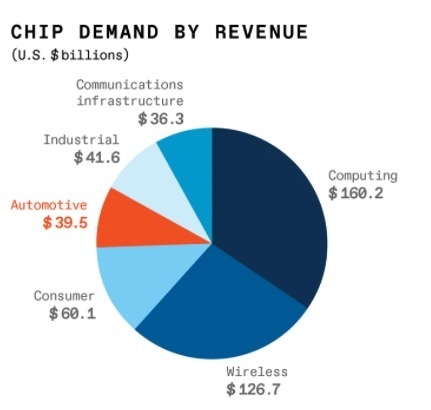
At $39.5 billion, the auto industry makes up less than 9 percent of chip demand by revenue according to International Data Corporation (IDC). That figure is set to increase by about 10 percent per year to 2025. However, the auto industry— which employs more than 10 million people globally— is something both consumers and politicians are acutely sensitive to, especially in the United States and Europe.
Chips for the automotive sector are made using processes intended to meet safety criteria that are different from those meant for other industries. But they are still fabricated on the same production lines as the analog ICs, power management chips, display drivers, microcontrollers, and sensors that go in everything else. The common denominator is the process technology is 40 nanometers and older. Cars rely on chips made using mature—40-nanometer and older—manufacturing processes. Those processes make up most of the installed capacity. This chip manufacturing technology was last cutting edge 15 years ago or earlier, lines producing chips at these old nodes represent a full 54 percent of installed capacity. Today these old nodes are typically used on 200-mm wafers of silicon. To reduce cost, the industry began moving to 300-mm wafers in 2000, but much of the old 200-mm infrastructure continued and even expanded.
Despite the auto industry’s desperation, there’s no great rush to build new 200-mm fabs. The return on investment just isn’t there. What’s more there are already many legacy-node plants in China that are not operating efficiently right now, but at some point, they will, further reducing the incentive to build new fabs. According to the chip manufacturing equipment industry association SEMI, the number of 200-mm fabs will go from 212 in 2020 to 222 in 2022, about half the expected increase of the more profitable 300-mm fabs.
More than 40 companies will increase capacity by more than 750,000 wafers-per-month from the beginning of 2020 to the end of 2022. The long-term trend to the end of 2024 is for a 17 percent increase in capacity for 200-mm facilities. Spending on equipment for these fabs is set to rise to $4.6 billion in 2021 after crossing the $3-billion mark in 2020 for the first time in years, SEMI says. But then spending will drop back to $4 billion in 2022. In comparison, spending to equip 300-mm fabs is expected to hit $78-billion in 2021.
_
According to an analysis by Goldman Sachs (GS), the semiconductor shortage touches a mind-blowing 169 industries in some way with automotive and consumer electronics industries among the most affected by the crisis. We’re talking everything from steel product and ready-mix concrete manufacturing to industries that build air conditioning systems and refrigerators to breweries. Even soap manufacturing is impacted by the chip crisis. To determine which industries were hit by the shortage, Goldman Sachs looked at each industry’s’ need for microchips and related components as a share of their GDP. Industries that spend more than 1% of their GDP on chips, the firm says, will be impacted by the semiconductor shortfall. For reference, in the automotive sector, 4.7% of industry GDP is spent on microchips and related semiconductors, on this basis, according to Goldman.
The automotive industry has been particularly burned by the chip shortage due to the way its supply chain works. Automakers tend to run incredibly lean on supplies for vehicles to keep costs down. But the coronavirus pandemic upended that entire system. When the pandemic began, automakers, figuring consumers would slow down auto purchases, cut down on their supplies of semiconductors used in everything from their vehicles’ infotainment systems to high-end driver-assistance technologies. But consumer interest in vehicle purchases rebounded faster than the automakers had predicted. And by Q4 of 2020, they were outpacing Q4 2019 sales numbers. At the same time factories remained idling due to coronavirus restrictions, putting automakers even further behind.
While that was happening, people around the world began buying up consumer technology goods to adjust to the pandemic induced work-from-home and remote learning environments. With automakers not purchasing chips, semiconductor makers started working on chips for consumer tech products. Once the automakers realized they needed more chips than they thought, the chipmakers were already dedicating time to making chips for consumer tech companies. Now both industries are struggling for support from the limited number of global semiconductor manufacturers that can meet their needs.
Chips aren’t exactly easy to make either, with advanced semiconductors taking up to 6 months to produce. According to Goldman Sachs’ Spencer Hill, the semiconductor shortfall could wallop U.S. GDP by as much as 1%, despite the uptick in consumer spending as lockdown orders continue to ease. “Some computer chips have no available substitute, and if output of every product that uses chips were to decline proportionately, the drag on 2021 GDP would be around 1%,” Hill wrote in a research note. While that prediction may sound dire, Hill says the true impact on GDP will likely be milder, with GDP taking a 0.5%, as companies that are able to use different available chips make adjustments to their needs.
The chip crisis is still far from over, however, and as industry leaders and politicians work to ease the strain on manufacturers across the country, consumer goods will still cost more as a result, with Goldman predicting a 1% to 3% jumping in prices.
_______
Sectors impacted by global chip shortage:
-1. Cars:
The average modern car can have between 1,400 and 1,500 chips, some even up to 3,000. Cars account for 15% of global chip production, while personal electronics account for around 50%. Chip revenues are even more skewed towards non-automotive sectors. The chip shortage is expected to cost the global automotive industry US$210 billion in revenue in 2021. Despite lower sales, some manufacturers increased profits over 2020, as General Motors, for example, saw record profits for 2021, due to resilient demand and decreased financial incentives offered to buyers.
At the start of the pandemic, car manufacturers incorrectly predicted that sales would drop, cancelled chip orders, and were unprepared to meet demand. Chip manufacturers had more commitments from the IT sector, which reduced capacity for car chips. Ford parked thousands of unfinished vehicles at Kentucky Speedway as the company waited for chips to finish assembling those cars. Toyota planned to cut vehicle production worldwide by 40% in September 2021, while General Motors announced it would halt production of almost all cars at its North American plants for a week or two that same month. During the third quarter of 2021, there were only two-thirds as many new car sales in the United States as there had been during the same time period in 2020, as supply could not meet demand. Opel closed its Eisenach manufacturing plant until 2022 because of the shortage, causing 1,300 workers to be temporarily laid off. As many as 9.4 million cars, or more than a tenth of the industry’s pre-pandemic output, could be eliminated from production plans.
What’s so special about one chip versus another? Why do automakers keep building more vehicles while half-finished cars and trucks sit waiting for chips? Because chips aren’t interchangeable, at least many of them aren’t. The chip you need to control seat heaters, for instance, is different from the one overseeing the power window, and neither is anything like the chips responsible for engine controls or safety systems. The hardware and software on each chip are not interchangeable. You can’t swap one out for another. They’re not compatible.
-2. Consumer Electronics:
Some experts blame the chip shortage in the automotive industry on the rapidly increasing demand for consumer electronics, particularly during the pandemic. In the meantime, the shortage could lead to lower profitability for the companies or raise consumer prices, which means more people may not be able to afford the goods. The consumer electronics industry scooped many of those chips up, but even so, makers of everything from laptops and TVs to gaming consoles and smartphones are raising prices due to tight supply, according to Vox. Although brands love to brag about their latest highly advanced chips, consumer electronics still can’t function without simple semiconductors. Just one example is HP, which raised the price of printers by 20% on average in a single year, according to the Wall Street Journal. Bloomberg reported that Sony won’t produce adequate supplies of its PlayStation 5 console until at least 2022.
Graphics cards and gaming PCs:
The global chip shortage made it difficult to acquire new graphics cards, while an increase in cryptocurrency mining in 2021 increased the demand even more. Finding gaming PC components became more difficult and more expensive, and as gaming PCs rely on either AMD or Nvidia to make their discrete GPU cards, both of those companies refreshed their line-ups during the pandemic with popular new models that are very difficult to find, or priced up to 300% above MSRP.
Video game consoles:
During the COVID-19 pandemic, cinemas and theaters were closed to prevent the spread of the virus, leading many people to turn to home entertainment during periods of self-isolation, which increased the demand for video game consoles. With the release of the ninth generation of video game consoles coinciding with the pandemic, demand increased even further, with both Microsoft and Sony reporting record demand for their new consoles. Microsoft expected in February 2021 that shortages of the Xbox Series X and Series S would continue until at least mid-2021, while Sony warned in May 2021 that short supply of the PlayStation 5 console would continue into 2022. Both companies use AMD chips manufactured by TSMC in their ninth-generation consoles, which puts extra strain on the supply chain.
-3. Appliances:
It’s not just cars and phones that can’t work without the chip-dependent computers that power them. Your dishwasher, refrigerator, freezer and microwave are all pretty much useless without semiconductors too — even if they’re not particularly sophisticated. Whirpool’s China operation was buckling under a 10% chip shortage. The company was struggling to meet domestic demand for appliances and a crush of new orders for exports at the same time.
-4. LEDs & Lighting Fixtures:
The chip shortage also affected LED supply. According to recent reports, the COVID-19 pandemic slowed down or even stopped construction, remodeling, and improvement for residential and commercial properties. This means that the demand for smart homes also slightly declined. Along with it, there’s not much demand for light-emitting-diode (LED) lights, which are considered to be a more sustainable option than halogen, incandescent, and fluorescent. For this market segment, there’s less likely to be a chip shortage. Instead, the prices for this raw material could go down, making the product more cost-effective and competitive. However, it is a different story for mini LED lights, which are currently used in many appliances and consumer electronics (such as televisions and smartphones). Apple and Samsung were preparing to debut their latest laptops, tablets and TVs and they all had one thing in common — they were all equipped with mini LED backlights powered by chips that were increasingly hard to find.
-5. Power-Turbines and Solar:
While most options for renewable energy are made of steel or aluminum, a part of their inner workings is controlled or managed by electronic parts, like semiconductors and sensors. And as expected, the chip shortage could mean a heavy blow for this growing industry.
_______
_______
Why aren’t there more semiconductor manufacturers? Why not increase chip production?
There is both a simple answer and a complicated one. The simple version is that making chips is incredibly difficult—and getting tougher. It’s not rocket science—it’s much more difficult. The more complicated answer is that it takes years to build semiconductor fabrication facilities and billions of dollars—and even then the economics are so brutal that you can lose out if your manufacturing expertise is a fraction behind the competition. This is why countries face such difficulty in achieving semiconductor self-sufficiency. China has called chip independence a top national priority in its latest five-year plan, while U.S. President Joe Biden has vowed to build a secure American supply chain by reviving domestic manufacturing. Even the European Union is mulling measures to make its own chips. But success is anything but assured. Manufacturing a chip typically takes more than three months and involves giant factories, dust-free rooms, multi-million-dollar machines, molten tin and lasers. The end goal is to transform wafers of silicon—an element extracted from plain sand—into a network of billions of tiny switches called transistors that form the basis of the circuitry that will eventually give a phone, computer, car, washing machine or satellite crucial capabilities.
_
Building semiconductor chips is an extremely complex, expensive and time-consuming process. For that reason, there are only a handful of chip manufacturers in the world. And all of those manufacturers are currently operating at full capacity. Adding new manufacturing facilities, also called foundries, takes years of planning and billions of dollars in investment. And even if these foundries had the capacity to build new chips, the process of doing so takes time. According to the Semiconductor Industry Association, it takes about 12 weeks to manufacture an average semiconductor. Advanced chips can take up to 20 weeks to build! Add in time to ramp up production and transport the finished product, and it’s estimated that the lead time for a new chip order is about six months.
_
Semiconductor manufacturers can supply any product’s increased demand if manufacturing capacity is sufficient. However, manufacturing semiconductor chips is a difficult, time-consuming, and expensive process that barriers players. Currently, the semiconductor industry is dominated by three manufacturers: Taiwan Semiconductor Manufacturing Company (TSMC), Intel, and Samsung.
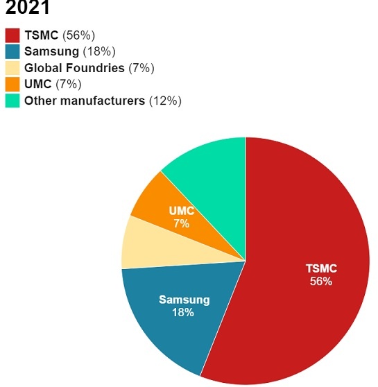
The current shortage highlights the fragility of this system and how easily production can be slowed by, say, a freak snowstorm. The cold snap in Texas saw electricity shortages, which led to Samsung halting production at its Austin chip foundry.
_
Chipmaking is a high-volume business that calls for incredible precision, along with making huge long-term bets in a field subject to rapid change. Chips are made in plants that cost billions to build and equip. They have to run flat-out 24/7 to recoup their investment. But it’s not just that. Yield, or the amount of good chips per batch, determines success or failure. It takes years of know-how and experience to get a yield of 90% out of the complex photolithographic process used to make chips. Imagine Ford Motor Co. being happy to throw away one car in 10. But chipmakers, who make millions of chips in a process that takes three to four months to complete, are successful if they’re hitting that mark. A foundry gobbles up enormous amounts of water and electricity and is vulnerable to even the tiniest disruptions (whether from dust particles or distant earthquakes).
_
Auto makers need chip makers, but the inverse isn’t true. The auto market as a whole accounts for less than 9 per cent of the entire semiconductor market in terms of consumption. Apple spends $56 billion a year on chips, compared to the $4 billion spent by the largest auto makers, such as Toyota. When chip makers decide which orders to meet, they choose the biggest customers. And even if they did choose the car makers, the process of etching billions of circuits onto a single wafer of silicon can take 26 weeks, or half a year. As a result, chip makers can’t rapidly meet auto makers’ demands.
__
The current chip shortage is unlikely to be resolved in the near future, partly because of the complexities of the semiconductor production process. Typical lead times can exceed four months for products that are already well established in a manufacturing line. Increasing capacity by moving a product to another manufacturing site usually adds another six months (even in existing plants). Switching to a different manufacturer typically adds another year or more because the chip’s design requires alterations to match the specific manufacturing processes of the new partner. And some chips can contain manufacturer-specific intellectual property that may require alterations or licensing.
______
______
Governments are worried:
Chips are now such a crucial component in many strategic technologies – from defense systems to cybersecurity to renewable energy – that their manufacture has become a big geopolitical issue: policymakers say that “chips are the new oil”. They were invented in the US, and much of the cutting-edge design still takes place there, but around 80% of production now happens in Asia because costs are lower: mostly in Taiwan, South Korea and China. The world’s biggest producer by volume is TSMC in Taiwan. Intel, based in California, is the biggest by revenue. Along with South Korea’s Samsung, these companies dominate high-end, specialised chips. But China is positioned to become the largest producer by 2030: its latest five-year plan sets the goal of meeting 70% of its semiconductor needs by 2025. Europe accounts for less than 10% of global chip production.
Recently the US Senate passed the Innovation and Competition Act, a $250bn bill designed to boost US semiconductor production, along with scientific research and other strategic technologies. The European Commission set out an ambitious plan to grow its share of the global semiconductor market to 20% by 2030, and committed $160bn of its Covid recovery fund to tech projects. The UK has long had a strong presence in the design side of the industry, but few producers; Newport Wafer Fab, the UK’s largest chip producer, has been acquired by Nexperia, a Chinese-owned company.
_______
_______
What is being done to ease the global chip shortage?
Companies try to remedy the ongoing saga of the lacking semiconductors and sensors by stockpiling as much as they can, but doing so may also leave other businesses, especially small ones, with nothing. The best solution is a combination of approaches that range from better diplomatic ties, a resilient supply chain, better inventory planning, stronger relationships with vendors, and even sound economic and trade policies.
_
The chip shortage is happening simultaneously with national and regional efforts to boost advanced logic chip manufacturing. South Korea announced a push worth $450-billion over ten years, the United States is pushing legislation worth $250 billion, and the EU could plow up to $160-billion into its semiconductor sector. Chipmakers were already on a spending spree. Globally, capital equipment for semiconductor production grew 56 percent year-on-year through April 2021, according to SEMI. Semiconductor Equipment and Materials International (SEMI) is a trade organization for the semiconductor and general electronics industry. SEMI’s 3 June 2021 World Fab Forecast indicates that 10 new 300-mm fabs will start operation in 2021 with 14 more coming up in 2022. The push for building IC capacity around the world will certainly drive fab investment of the current decade to a new high.
With demand for semiconductors expected to grow as more industries embrace digital transformation, chip manufacturers and governments collaborate to expand supply networks’ capacity. As the virus continues to spread around the world, the chip industry is preparing for the post-pandemic period with billions of dollars in investments to buck the crisis. As companies and countries are trying to shape the chip industry with huge investments, it was recently announced that Intel, one of the world’s largest chipmakers, plans to build two new chip factories in the US state of Arizona with an investment of $20 billion. South Korean electronics giant Samsung is also laying out $116 billion with the goal of becoming the largest chipmaker by 2030. Towards that end, a giant Samsung factory under construction in northwestern South Korea is expected to start production this year. Taiwan Semiconductor Manufacturing (TSMC), the world’s largest contract manufacturer, is also building a $12 billion factory in Arizona like Intel. The factory is expected to start production in 2024. In China, which wants to cut its dependence on foreign chips, two national wealth funds provided a total of $2.25 billion to SMIC, the country’s leading chip manufacturer, to boost production at its factory in Shanghai.
__
Self-sufficiency:
Can you really move the whole electronics industry to one country the US?
No way. The electronics industry is vastly larger than just making chips, including upstream supplies like wafers and manufacturing equipment and downstream activities like packaging, testing and assembly, most of it in Asia. There’s a lot of other aspects of the supply chain, those need to be more balanced as well. Nearshoring, which would move manufacturing operations nearer to the US but not all the way, is another possibility, particularly for assembly, testing and other work not quite as high-tech as the chipmaking itself.
The Boston Consulting Group expects it would take $900 billion to $1.23 trillion in spending to create self-sufficient semiconductor supply chains worldwide. For just the US, it’s $350 billion to $420 billion. And that cost runs contrary to the capitalistic impulse to reward the least expensive suppliers.
Boston Consulting Group semiconductor study:
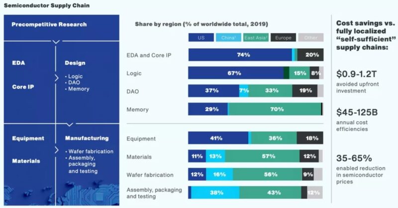
Different regions develop specialties in semiconductor manufacturing around the world, and reproducing that expertise locally would cost $900 billion to $1.2 trillion, says a Boston Consulting Group study.
TSMC founder and former CEO Morris Chang is skeptical. “It’s not going to be possible to turn back the clock,” Chang said. “If you want to re-establish a complete semiconductor supply chain in the United States, you will not find it to be a possible task.”
Chip players naturally clump into “highly concentrated clusters,” consulting firm Deloitte said in a report. Spreading that work geographically will help supply chain woes, but it’s not easy. “Clusters create strong pools of talent and skills. Prior attempts to build more geographically distributed manufacturing capacity (such as Silicon Glen in the United Kingdom in the late 1970s) came to naught,” Deloitte concluded.
The Massachusetts Institute of Technology believes investments need to happen at the research level, not just with chipmakers. The hollowing out of semiconductor manufacturing in the US is compromising our ability to innovate in this space and puts at risk our command of the next technological revolution. To ensure long-term leadership, leading-edge semiconductor manufacturing in the US must be prioritized and universities activities have to get closer to it, MIT said in a report. It called for upgrades from 1990s-era technology that tiles chips onto silicon wafers 150mm in diameter to equipment with 200mm wafers that are newer if not cutting edge.
_____
_____
When will the global chip shortage end?
How long the chip shortage will last depend on who is doing the forecasting. Gartner has estimated that the semiconductor shortage will extend well into 2022 and has warned that there could be a year’s lead time for wafer orders. Forrester said it expects the chip shortage to continue through 2022 and into 2023.
Supply will grow “from older chip fabs and foundries running processes far from the cutting edge and on comparatively small silicon wafers,” wrote the IEEE. More than 40 companies will increase capacity by more than 750,000 wafers per month to the end of 2022, the IEEE said.
Despite a reluctance by some manufacturers to build new plants, there has been momentum. Intel said it will spend $20 billion to build two new fabs in Arizona, and TSMC plans to spend $28 billion on new chips and building plants to increase capacity. Texas Instruments announced in November 2021 plans to build as many as four new semiconductor plants in Texas at an estimated $30 billion. Construction on the first two fabrication plants is slated to begin in 2022, and production of TI’s 300-millimeter wafers is expected to start by 2025, according to the company. TI will have the option to build out two additional plants at the site in the future. With Samsung announcing it will build a $17 billion plant starting in 2022, other states and cities around the country are trying to woo the company with incentives in the hope of attracting chip production to their areas.
In terms of federal efforts, the Senate in June 2021 passed a $250 billion spending bill—one of the largest industrial bills in U.S. history—which included $54 billion to increase production and research into semiconductors. However, five months later, the legislation has stalled in the House of Representatives because House members said they want to write their own bill. U.S. House and Senate lawmakers said recently that they have chosen negotiators to hammer out a deal on a bill to provide $52 billion in government subsidies for semiconductor production after months of discussion. Experts have said the U.S. could be at a strategic disadvantage in the years ahead if semiconductor production is not expanded in the country.
__
There is no end in sight. Intel’s chief executive, Pat Gelsinger, said that he thinks it could be two years before production is able to ramp up. “The shortage will probably continue for a few years,” said Michael Dell, chief executive of Dell Technologies, earlier in the year. On the other hand, Nvidia CEO Jensen Huang stated that he anticipates the shortfall to last far into 2022, while AMD CEO Lisa Su stated that the deficit will improve in the second half of 2022. However, supply would remain tight until then. IBM CEO Arvind Krishna stated that “More than likely, the chip shortage will continue until 2023 or 2024 at the earliest.” The likes of TSMC, Samsung and Intel are all investing heavily. But “even if chip factories are built all over the world, it takes time”, says Dell. Many companies are examining their supply chains: Tesla is considering buying a chip plant outright. High-tech industries will probably recover first, towards the end of this year. Cars and home appliances, which use cheaper, older chips will take longer: they are not so profitable for manufacturers, so there is not the impetus for them to invest. Product delays and parts shortages will continue for some time. Analysts believe that the worldwide chip deficit could stretch throughout the next year and maybe into 2023. The shortage is because current capacity expenditures will take fruit,” said Malcolm Penn, CEO of industry researcher Future Horizons. Even if the current global chip shortfall is resolved, it is possible that other supply issues will arise as the demand for electronics continues to grow.
______
The microchip crisis will intensify: experts say:
Analysts have been closely monitoring the car industry and cut more than 5 million cars in the forecast for global production this year 2022 and next, largely due to the expected consequences of Russia’s invasion of Ukraine. S&P Global Mobility, formerly known as IHS Markit, has reduced its estimates for 2022 and 2023 by 2.6 million vehicles each. Experts now expect carmakers to produce 81.6 million cars worldwide this year and 88.5 million next year. S&P Global Mobility mentions the effect of the Russian war on energy and commodity prices, expectations that the semiconductor deficit will worsen, and disruptions to the wiring flow in Ukraine. Suppliers may have problems with the supply of neon gas used to make chips in Ukraine, as well as palladium in Russia. Although low in probability, the palladium has the potential to become the industry’s biggest supply constraint. Russia produces 40% of the world’s palladium, according to the US Geological Survey. About two-thirds of palladium use is in vehicles, where it is the active ingredient in catalytic converters for exhaust gas aftertreatment. If the supply of Russian palladium were abruptly cut off, the production of all vehicles using such sources could stop. Although platinum is an alternative, it is just as expensive and is also mostly from Russia.
_______
_______
Section-14
Chip research:
Innovation doesn’t stop when transistor shrink is no longer feasible. It just becomes more challenging, and, as a result, more profitable if done well. These next-generation chip designs will include more exotic materials, new packaging technologies and more complex 3D designs. While the utilization of new materials can help to engineer new and more powerful, computer systems, there are a number of other innovations that chip manufacturers are dabbling with, such as using a 3D, upwards pattern for packing transistors on integrated circuit boards, and the utilization of novel Rare Earth Elements for the manufacturing of computer chips. The semiconductor industry will connect engineers from across the entire breadth of physical, chemical, biological and computer sciences in order to realize these new designs. When (and not if) they do, the designs will help to generate consumer products that right now we can’t even conceive of. They will also enable the next big waves of innovation that are on the horizon, such as automated transportation, advanced AI and fast connectivity with 5G.
_____
New semiconductor materials:
Although silicon might be used extensively for computer chips, owing to certain limitations alternatives are being worked upon. Silicon chips are only economical if they are tiny. Silicon furnaces are becoming 10 times more expensive every several years. Furthermore, it is hard to reconcile with other elements in a timely and cost-effective manner. Isolated silicon atoms have a physically demanding limit (about 0.2nm), yet their activity becomes unpredictable and hard to sustain under certain conditions. Without the potential to further downsize ICs, silicon cannot continue to produce the benefits it has thus far.
The semiconductor industry today is mostly based on silicon and silicon oxide. These are materials with very good electronic properties. For a long time, ever thinner layers of these materials were used to miniaturize electronic components. This worked well for a long time—but at some point we reach a natural limit. When the silicon layer is only a few nanometers thick, so that it only consists of a few atomic layers, then the electronic properties of the material deteriorate very significantly. The surface of a material behaves differently from the bulk of the material—and if the entire object is practically only made up of surfaces and no longer has a bulk at all, it can have completely different material properties. Therefore, one has to switch to other materials in order to create ultra-thin electronic components. And this is where the so-called 2D materials come into play: they combine excellent electronic properties with minimal thickness.
2D materials:
In materials science, the term single-layer materials or 2D materials refers to crystalline solids consisting of a single layer of atoms. These materials are promising for some applications but remain the focus of research.
Chip-scale embedded electronics, which have a small footprint, reduced energy requirement, and inexpensive production due to widespread production, have had a significant impact on our modern lifestyles. Although traditional metal-oxide-semiconductors, such as silicon, have influenced embedded devices, they incur several inherent material restrictions. Other material integrations on-chip has shown to be an appealing method for overcoming these issues.
Since the ground-breaking development of nanoparticles such as graphene, 2D multi-layered materials have piqued the majority’s curiosity, and the material category is fast expanding. When compared to bulk counterparts, 2D alternatives have numerous exceptional qualities, including ultra-high charge transport, layered sensitive bandgaps, significant asymmetry, bandwidth, minimal photonic scattering, and outstanding nonlinear absorption characteristics.
Their inherent thin shape further benefits high-density integration and low-power performance. The use of 2D materials on traditional electronic components such as computer chips combines the perfect combination.
The advantageous 2D materials include graphene, graphene oxide, transition metal dichalcogenides, black phosphorus as well as hexagonal boron nitride, Mxenes, perovskites, and metal-organic frameworks. These materials have been used for thin films, microchips, field-effect transistors, micro-supercapacitors, and energy storage materials.
Graphene Processors:
Graphene is the new, major player in the world of materials science, and is a very thin, flexible – but incredibly strong – zero overlap semimetal that is also a very powerful conductor. As a possible candidate for use in computers, graphene can be used to make computers more powerful and fast when used in computer processors, and to date, IBM has already used the novel material to create a chip that is 10,000 times faster than normal chips.
Carbon Nanotube Chips:
Researchers focused on carbon nanotubes for the fabrication of computer microchips as they offer major benefits in terms of energy consumption. They also transport electrical charges substantially well. As a result, they produce superior semiconductor transistors as compared to silicon. Carbon nanotube electronics might theoretically be three times better than silicon computer chips in terms of processing speed. They would also use around one-third of the energy that silicon processors use.
Nanomagnetic Chips:
Nanomagnetic chips are made from material similar to refrigerator magnets, etched with rows of rectangles. Each rectangle measures about 100 nanometers on a side and has magnetic poles. Information is stored in how they point: One configuration is 1, the other is 0. Because the magnets are so small, they can be packed close enough for their magnetic fields to interact. Information passes without any physical changes to the chip. Nanomagnets employ nanomagnetic technology to convey and process data. They do this by utilizing switchable magnetic modes that are photolithographically adhered to the system networks of a circuit. Nanomagnetic logic functions similarly to silicon-based semiconductors, except instead of turning transistors on and off to generate binary data, magnetization levels are switched. This binary data may be interpreted via dipole-dipole couplings (the connection among each magnet’s north and south poles). Nanomagnetic logic consumes relatively little power since it does not depend on an electrical current. When environmental issues are taken into account, this renders them the appropriate substitute.
Apart from the above-mentioned materials, zeolite thin film micro-chips are also being researched owing to their low dielectric constant and superior efficiency.
A novel semiconducting material with high thermal conductivity can be integrated into high-power computer chips to cool them down and so improve their performance. The material, boron arsenide, is better at removing heat than the best thermal-management devices available today.
Scientists are developing computing devices built from living organisms such as slime mould and bacteria, in order to harness their problem-solving and programmable properties.
_______
_______
New Chip Architecture combines logic and memory:
It’s a major breakthrough in the field of electronics. Engineers at EPFL’s Laboratory of Nanoscale Electronics and Structures (LANES) have developed a next-generation circuit that allows for smaller, faster and more energy-efficient devices — which would have major benefits for artificial-intelligence systems. Their revolutionary technology is the first to use a 2D material for what’s called a logic-in-memory architecture, or a single architecture that combines logic operations with a memory function. The research team’s findings appear in Nature.
Until now, the energy efficiency of computer chips has been limited by the von Neumann architecture they currently use, where data processing and data storage take place in two separate units. That means data must constantly be transferred between the two units, using up a considerable amount of time and energy. By combining the two units into a single structure, engineers can reduce these losses. That’s the idea behind the new chip developed at EPFL, although it goes one step beyond existing logic-in-memory devices. The EPFL chip is made from Molybdenum disulfide (MoS2), which is a 2D material consisting of a single layer that’s only three atoms thick. It’s also an excellent semi-conductor. LANES engineers had already studied the specific properties of MoS2 a few years ago, finding that it is particularly well-suited to electronics applications. Now the team has taken that initial research further to create their next-generation technology.
The EPFL chip is based on floating-gate field-effect transistors (FGFETs). The advantage of these transistors is that they can hold electric charges for long periods; they are typically used in flash memory systems for cameras, smartphones and computers. The unique electrical proprieties of MoS2 make it particularly sensitive to charges stored in FGFETs, which is what enabled the LANES engineers to develop circuits that work as both memory storage units and programmable transistors. By using MoS2, they were able to incorporate numerous processing functions into a single circuit and then change them as desired.
This ability for circuits to perform two functions is similar to how the human brain works, where neurons are involved in both storing memories and conducting mental calculations. This circuit design has several advantages. It can reduce the energy loss associated with transferring data between memory units and processors, cut the amount of time needed for computing operations and shrink the amount of space required. That opens the door to devices that are smaller, more powerful and more energy efficient. This technology is particularly promising for applications relying on artificial intelligence.
______
______
Vertical transistors:
Semiconductor chips contain tiny gates called “transistors” that control the flow of electricity. This is what allows a traditional computer to process information, using a binary on/off code. (If a gate’s open, that’s a “1.” If it’s closed, that’s a “0.”) To make faster, more powerful computers, we need microchips with more transistors, but to keep the chips, well, micro, we’ve had to keep packing more and more transistors into the same area. We’re now hitting a wall in the amount of transistors we can pack onto a microchip. Making them smaller is just becoming physically impossible. The fact is, when they’re talking about building physical entities like semiconductors and transistors, you can only go so small. Atoms have a certain size, and you’re approaching the almost atomic molecular distances at this point and you’re limited by that.
IBM and Samsung have unveiled a new microchip design that promises radically faster, more efficient chips. IBM and Samsung’s new design stacks transistor components vertically on a microchip, with electricity flowing up and down, rather than the traditional horizontal design, with electricity flowing from side to side. They call their approach “Vertical-Transport Field Effect Transistor” (VTFET), and they say it could not only allow for more transistors on a microchip, but also make the flow of electricity through them more efficient.
_
Historically, transistors have been built to lie flat upon the surface of a semiconductor, with the electric current flowing laterally, or side-to-side, through them. With new Vertical Transport Field Effect Transistors, or VTFET, IBM and Samsung have successfully implemented transistors that are built perpendicular to the surface of the chip with a vertical, or up-and-down, current flow.
The DNA of any hardware technology is the transistor. Billions of transistors can cover the surface of a silicon wafer, and these wafers are layered together to make a microchip. A typical, standard transistor that’s commonly found in electronics has three terminals: source, gate, drain. The current (which is a stream of electrons) flows from source to drain. The gates control the flow of currents and dictate the state of the transistor. When voltage is applied to the gate, the transistor is turned on and in state 1. When no current is flowing between the source and drain, the state is 0. Additionally, two separate transistors need a region in between to isolate them and prevent them from interfering with one another, and this is done with dummy gates. Then there is a concept called “contacted gate pitch” which is the physical distance required to fit all the transistor components. These are very basic structural requirements, and you can think of two hard walls and you have to fit the gate, the spacer, and the region for contact within that. The walls keep closing in, but at some point, they can’t come any closer without sacrificing functionality.
Previous transistor innovations like FinFETs and nanosheets, have the gate, source, and drain on the same plane. With a vertical design, these structures essentially get stacked on top of each other, on the wafer. Plus, vertical transistors don’t need a dummy gate—they instead use something called shallow trench isolation, which conserves space. They also flip the orientation of the current flow, which still flows from the source to the drain, but now is perpendicular to the surface of the wafer instead of in parallel. By doing this change, you now can independently change the gate length, spacer thickness, and the contacts. Because you’re able to go vertically and pack these transistors even closer together, you’re now able to get more transistors in a given area.
Compared to today’s best 3D transistor technology (like FinFET), the VTFET can allow them to squeeze up to five times more transistors in a chip of the same size. This is useful in applications where the size of the chip is fixed. In testing, compared to a FinFET device of the same scale, IBM claims to have observed a 50 percent reduction in capacitance and in resistance, which reduced power use by 85 percent.
Transistor design has been overhauled again and again over the last 80 years. The FinFET model improved upon a design called MOSFET from the 1960s. A few years ago, an architecture called a nanosheet with a gate all around the transistor made devices less leaky. FinFET transistors consist of a fin-shaped channel surrounded on three sides by a “gate” that controls the flow of electrons. But IBM’s nanosheet (or gate-all-around) transistors have a layered channel instead. The layers are stacked on top of each other and, like three pigs-in-a-blanket, are surrounded by the gate on all sides. This last bit is the most critical piece. Gate-all-around transistors provide better control of current through the channel, prevent leakage, and boost efficiency.
High-K metal gates took 16 years to get to the manufacturing stage. FinFET took the industry about 14 years to get to manufacturing. Nanosheet, which many groups are still tinkering with, has not reached the manufacturing stage yet, but is expected to in the next two years. After that, it will take about 14 more years until it’s introduced into everyday electronic devices. Researchers are talking about VTFET today, not two years from now, because this innovation is such an important breakthrough. They are asking the industry to look at this new technology offering and enable better processes, better design tools around this innovation, so that semiconductor community can truly utilize this technology feature in five to eight years.
______
______
New chip design pushes computing to the edge:
Princeton researchers have created a new chip that speeds artificial intelligence systems called neural nets while slashing power use. The chips could help bring advanced applications to remote devices such as cars and smartphones. By cutting both power demand and the need to exchange data from remote servers, systems made with the Princeton technology will be able to bring artificial intelligence applications, such as piloting software for drones or advanced language translators, to the very edge of computing infrastructure. To make AI accessible to the real-time and often personal process all around us, we need to address latency and privacy by moving the computation itself to the edge. And that requires both energy efficiency and performance.
Ideally, the computation for technology such as drone navigation would be based on the drone itself, rather than in a remote network computer. But digital microchips’ power demand and need for memory storage can make designing such a system difficult. Typically, the solution places much of the computation and memory on a remote server, which communicates wirelessly with the drone. But this adds to the demands on the communications system, and it introduces security problems and delays in sending instructions to the drone. The new chip is based on analog computing, which uses circuits to mimic equations being solved rather than generate 1s and 0s like a digital computer.
Analog computing was the dominant technology through the Second World War. It was used to perform functions from predicting tides to directing naval guns. But analog systems were cumbersome to build and usually required highly trained operators. After the emergence of the transistor, digital systems proved more efficient and adaptable. But new technologies and new circuit designs have allowed engineers to eliminate many shortcomings of the analog systems. For applications such as neural networks, the analog systems offer real advantages. Now, the question is how to combine the best of both worlds. Digital systems play a central role while neural networks using analog chips can run specialized operations extremely fast and efficiently. That is why developing a software system that can integrate the two technologies seamlessly and efficiently is such a critical step.
_____
_____
Flying Chips:
The chips may be the smallest ever human-designed flying machines. Winged microchips each about the size of a grain of sand may be the smallest-ever artificial flying structures, devices that could one day help monitor air pollution and airborne disease. The new chips, or “microfliers,” are not equipped with motors or engines. Instead, much like a maple tree’s propeller seed, they fly on the wind, twirling like helicopter blades through the air toward the ground. By analyzing the aerodynamics of wind-dispersed seeds and modeling how air flows around these microfliers, the scientists pinpointed the ideal structures for slow, controlled flight. Their design helps ensure the microfliers disperse over a broad area and stay aloft for a long time to better monitor the air.
The scientists could integrate a variety of electronics into the microchips, including circuits to detect airborne particles, sensors to monitor water quality, light detectors to measure sunlight, electronics to harvest and store energy from light, a CPU and memory, and an antenna to wirelessly transfer data to a smartphone, tablet or computer. The microfliers can serve as a dispersed network of sensitive environmental sensors for monitoring contamination, study population movement, or track the spread of disease. Manufacturing them from benign, biodegradable materials would provide a way to collect detailed, high-resolution data using a platform that vanishes harmlessly into the environment.
_____
_____
3D chips with transistors made of carbon nanotubes:
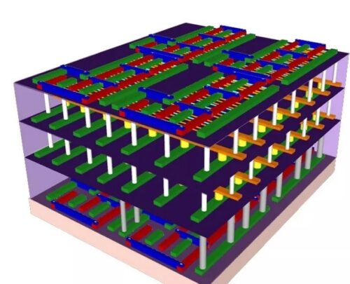
Figure above shows carbon nanotube stacked 3D chip.
_
Carbon nanotubes (CNTs) are hollow cylinders composed of a single sheet of carbon atoms. They have exceptional properties which make them ideal as a semiconductor material for building transistors, the on-off switches at the heart of electronics. CNTs are so thin – thousands could fit side-by-side in a human hair – that it takes very little energy to switch them off. Carbon nanotubes (CNT) are miniscule mesh rods made of carbon atoms that have electrical properties similar to those of conventional silicon transistors. The new chips are not yet ready to unseat silicon ones in modern electronics. Each carbon transistor is about a millionth of a meter across. At a width of eight microns (8,000 nanometers) they are much fatter than today’s most advanced silicon chips. Current silicon transistors are smaller. They are tens of billionths of a meter across. Each carbon-nanotube transistor in this prototype can flip on and off about a million times a second. Silicon transistors can flicker billions of times per second. That puts nanotube transistors on a par with silicon transistors of the 1980s. In 2013, researchers built a CNT computer, which they described in the journal Nature. That computer, however, was slow and bulky, with relatively few transistors. The next step is to scale the system further, to make even bigger, more complicated chips. Shrinking the nanotube transistors would help electricity zip through them with less resistance. That would allow the devices to switch on and off faster. They could also align the nanotubes in parallel, rather than using a randomly oriented mesh. This could increase the electric current through the transistors. That would further boost processing speeds.
_
Researchers have created a system for stacking memory and transistor layers, with tiny wires connecting the two. The new design using carbon nanotubes allows memory and processor layers to be stacked in three dimensions. The new 3D design has slashed the transit time between transistor and memory, and the resulting architecture can produce lightning-fast computing speeds up to 1,000 times faster than would otherwise be possible. Companies today already make 3D chips with silicon as a way to pack logic and memory functions closer together to speed up processing. But the chips are slowed down by bulky and sparse wiring that carries information between the chip layers. And because 2D silicon chip layers must be fabricated separately at more than 1000°C, there is no way to build up 3D chips in an integrated fabrication plan without melting the lower layers. Carbon nanotube transistors, which can be made nearly at room temperature, offer a better path to dense, integrated 3D chips. The 3D design enables scientists to interweave memory, which stores data, and the number-crunching processors in the same tiny space. Reducing the distance between the two elements can dramatically reduce the time computers take to do their work.
______
______
3D curved microchips could pave way to more efficient “spintronic” computers:
Researchers from The University of Manchester, with colleagues from the universities of Groningen and Utrecht in the Netherlands, say 3D curved microchip structures could be used to develop more powerful – and energy efficient – spin-based computers. The work, published online in the journal Nano Letters, outlines the main challenges involved in creating 3D curved microchips that rely on the “spin” of electrons to carry and store information. According to Dr Ivan Vera-Marun, a lead researcher on the study, the key issue is that spin-based microchips are usually 2D structures. Therefore, a fundamental challenge when building 3D structures is transporting electrons without losing their unique spin properties. Collectively, the use of electron spin in electronics is known as “spintronics”.
To investigate this, the researchers used ion beams – a form of molecular sandblasting – to carve trenches in a piece of silicon, the material which forms the basis of microchips. They then grew nano-scale aluminium channels across these trenches, through which the electrons could travel. The movement of the electrons through these curved channels, and across the trenches, mimics the movement of electrons through a 3D structure with multiple layers of material. In doing so, the researchers hoped to discover what factors affect the spin and charge of electrons, characteristics which affect the efficiency and speed of electronic devices.
Arguably the most important finding to come from the paper is that the shape and varying thickness of the aluminium channels directly affected these characteristics. “What we discovered is that variations in the trench size would affect spin and charge transport in the channel differently,” explains Dr Kumar Sourav Das, then a PhD student supervised by Dr Vera-Marun. Dr Das added; “Thus, we could independently tune both spin and charge currents based on the channel geometry.” This could help to create more energy efficient electronics, as spintronics is an attractive way of creating low-power devices.
Spintronics are already used in memory storage, and the authors suggest a number of applications for this new research, including the possibility to use it as the basis for a new generation of quantum computer chips.
_____
_____
Technology that could end up replacing semiconductors all together:
It is widely predicted the doubling of silicon transistors per unit area every two years will come to an end around 2025 as the technology reaches its physical limits. However, researchers at RMIT University in Melbourne, Australia, believe a metal-based field emission air channel transistor (ACT) they have developed could maintain transistor doubling for another two decades.
The ACT device eliminates the need for semiconductors. Instead, it uses two in-plane symmetric metal electrodes (source and drain) separated by an air gap of fewer than 35 nano meters, and a bottom metal gate to tune the field emission. The nano scale air gap is less than the mean free path of electrons in the air; hence electrons can travel through the air under room temperature without scattering.
Unlike conventional transistors that have to sit in silicon bulk, their device is a bottom-to-top fabrication approach starting with a substrate. This enables them to build fully 3D transistor networks if they can define optimum air gaps. This essentially means they can stop pursuing miniaturization, and instead focus on compact 3D architecture, allowing more transistors per unit volume.
Using metal and air in place of semiconductors for the main components of the transistor has many other advantages, as well. Fabrication becomes essentially a single-step process of laying down the emitter and collector and defining the air gap. Although standard silicon fabrication processes are employed in producing ACT’s, the number of processing steps are far fewer, given that doping, thermal processing, oxidation, and silicide formation are unnecessary. Consequently, production costs should be cut significantly.
Replacing silicon with metal means these ACT devices can be fabricated on any dielectric surface, provided the underlying substrate allows useful modulation of emission current from source to drain with a bottom-gate field. Machines can be built on an ultra thin glass, plastics, and elastomers so that they could be used in flexible and wearable technologies.
_____
_____
Chips capable of imitating the way brain synapses work:
-1. Photonic microchip:
As artificial intelligence continues making machines smarter, many in the tech sector believe the “singularity” is right around the corner — the point of technological progress where machines are exponentially smarter than humans. But when it comes to computing, the human brain remains much more powerful (and more energy-efficient) than any technological processing system on the planet. In fact, developing microchips capable of imitating the way brain synapses work — particularly their ability to process and store information using almost no energy — has long been the holy grail of computing.
With a new innovation, scientists have moved one step closer to that goal. A team led by researchers from Exeter, Oxford, and Münster universities has developed specialized photonic microchips, which could one day help to create computers that can store and process huge amounts of information at faster speeds than the human brain can. Because the microchips are powered by light, they could also execute high-speed computing at a lower power supply than could ever be possible with any electronic processing system.
_
The human brain’s powerful hardware:
In the brain, synapses connect nerve cells (or neurons) to one another. The brain signals that form memories and thoughts move through these nerve cells as tiny electrical charges; when a charge reaches a synapse, it triggers the release of neurotransmitters, the chemical messengers that communicate information throughout the brain. Synapses are essentially the “circuits” that facilitate our thinking, feeling, and activation of movement. And there are plenty of them: with around 100 billion neurons existing in a healthy brain — and each one connected to thousands of others — estimates put the number of synapses in the brain between 100 trillion and 1,000 trillion. More amazing than their number, though, is their speed: the many trillions of “synaptic connections” in the brain operate at a speed akin to that of a computer with a 1 trillion bit per second processor. To date, even the world’s fastest processors and CPUs have been unable to come close to the processing speed of brain synapses. In one simulation, it took 40 minutes of work by over 80,000 processors in K computer — one of the fastest supercomputers on the planet — to achieve just 1 second of biological brain processing time.
Making computers faster is possible, but also demands more energy. That gives the human brain essentially two main components where it has the upper hand over machine. Our immense network of neurons and synapses can:
-1) rapidly process and store vast amounts of information simultaneously (this is known as “parallel processing”), and
-2) carry out parallel processing using very little energy totaling just a few tens of watts of power.
“Since synapses outnumber neurons in the brain by around 10,000 to 1, any brain-like computer needs to be able to replicate some form of synaptic mimic,” said Professor Wolfram Pernice, a co-author of the paper from the University of Münster. “That is what we have done here.”
With their light-powered microchip, the team of European researchers tackled both issues — creating a “hardware synapse” capable of incredible speed, that operates with incredibly little power. The team created the chip by combining “phase-change” materials commonly found in household items, such as rewriteable CDs and DVDs, with photonic integrated circuits. Phase-change materials are a class of substances capable of storing and releasing large amounts of energy in response to heat stimuli. Photonic integrated circuits, meanwhile, use light — rather than electrons — to manipulate atoms and perform other functions.
Using light in place of more expensive, inefficient energy sources (such as electricity) is a goal of many scientists. In fact, an entire discipline known as “integrated photonics” is focused on developing fast-processing microchips based on light signals for use in faster, greener electronics.
The photonic microchips developed by the Exeter, Oxford, and Münster researchers are a leading example. According to the team, their photonic synapses can operate at speeds a thousand times faster than those of the human brain — representing a crucial step toward unlocking the “holy grail” of brain-mimicking computers.
While the research team has so far only conducted tests to prove the microchip’s programmability and effectiveness in “synaptic mimic,” they say their brain-inspired innovation displays the essential requirements of a solution for a neuromorphic computing tool. And that is what potentially makes the photonic microchip, in the words of the researchers, such a “pioneering breakthrough.”
It comes back to AI: if a high-speed, light-based neurochip is developed into our electronics in the not-so-distant future, those devices will be able to process artificial intelligence algorithms at a faster, lower-energy clip than ever. If devices can support AI and conduct advanced machine learning faster, the human brain begins to lose some of its supremacy over the machine, perhaps putting us another step closer to the singularity.
_
-2. Neuromorphic chips:
Advances in machine learning have moved at a gallop in recent years, but the computer processors these programs run on have barely changed. To remedy this, companies have been re-tuning existing chip architecture to fit the demands of AI, but on the cutting edge of research, an entirely new approach is taking shape: remaking processors so they work more like our brains. This is called “neuromorphic computing,” and scientists from MIT said they’ve made significant progress in getting this new breed of chips up and running. Their research, published in the journal Nature Materials in 2018, could eventually lead to processors that run machine learning tasks with lower energy demands — up to 1,000 times less. This would enable us to give more devices AI abilities like voice and image recognition.
To understand what these researchers have done, you need to know a little about neuromorphic chips. The key difference between these processors and the ones used in your computer is that they process data in an analog, rather than a digital fashion. This means that instead of sending information in a series of on / off electrical bursts, they vary the intensity of these signals — just like our brain’s synapses do. This means that more information can be packed into each jolt, drastically reducing the amount of power needed. It’s like the difference between morse code and speech. The former encodes data using just two outputs, dots, and dashes — making meanings easy to understand but lengthy to communicate. Speech, by comparison, can be difficult to interpret (think fuzzy phone lines and noisy cafes) but each individual utterance holds much more data. A big difficulty with building neuromorphic chips, though, is being able to precisely control these analog signals. Their intensity needs to vary, yes, but in a controlled and consistent fashion.
Attempts to find a suitable medium for these varying electrical signals to travel through have previously been unsuccessful, because the current ends up spreading out all over the place. To fix this, researchers led by MIT’s Jeehwan Kim, used crystalline forms of silicon and germanium that resemble lattices at the microscopic level. Together, these create clear pathways for the electrical signals, leading to much less variance in the strength of the signals. “This is the most uniform device we could achieve, which is the key to demonstrating artificial neural networks,” Kim told MIT News.
To test this premise, Kim and his team created a simulation of their new chip design, with the same degree of variance in signals. Using it, they were able to train a neural network that could recognize handwriting (a standard training task for new forms of AI) with 95 percent accuracy. That’s less than the 97 percent baseline using existing algorithms and chips, but it’s promising for new technology.
There’s a long way to go before we’ll know whether neuromorphic chips are suitable for mass production and real-world usage. But when you’re trying to redesign how computers think from the ground up you have to put in a lot of work. Making sure neuromorphic chips are firing their electric synapses in order is just the start.
________
________
Memristors:
A memristor (named as a portmanteau of memory and resistor) is a non-volatile electronic memory device that was first theorized by Leon Ong Chua in 1971 as the fourth fundamental two-terminal circuit element following the resistor, the capacitor, and the inductor (IEEE Transactions on Circuit Theory, “Memristor-The missing circuit element”). Its special property is that its resistance can be programmed (resistor function) and subsequently remains stored (memory function). Unlike other memories that exist today in modern electronics, memristors are stable and remember their state even if the device loses power.
However, it was only almost 40 years later that the first practical device was fabricated. This was in 2008, when a group led by Stanley Williams at HP Research Labs realized that switching of the resistance between a conducting and less conducting state in metal-oxide thin-film devices was showing Leon Chua’s memristor behavior. Since then, the field has rapidly grown and there has been a huge amount of work in the area. Very high levels of endurance (120 billion cycles) and retention (10 years or more) have recently been achieved in memristor devices and ultrahigh density crossbar arrays, including multiple layer stacking, have been realized with scalability down to 2-10 nanometers.
Today, most computers use random access memory (RAM), which moves very quickly as a user works but does not retain unsaved data if power is lost. Flash drives, on the other hand, store information when they are not powered but work much slower. Memristors could provide a memory that is the best of both worlds: fast and reliable.
Memristors can help to transform future integrated circuits by acting alongside resistors, capacitors and transistors, by regulating electrical flow within a circuit (like a resistance switch) while remembering the amount of charge that had previously flown through it. In this way, it could act as non-volatile, resistive RAM (Random Access Memory) and could thus help to save on energy resources, and could one day replace flash memory.
______
______
Quantum Computing Chip:
Quantum physics is the theoretical basis of the silicon transistor that enabled the computing revolution. But on the algorithmic level, today’s computing machinery still operates on ‘classical’ Boolean logic. Quantum computing is the design of hardware and software that replaces Boolean logic by quantum law at the algorithmic level i.e., using superposition and entanglement to process information. Quantum computing is the use of quantum-mechanical phenomena such as superposition and entanglement to perform computation. Quantum computers rely on the physical properties of electrons, photons, and other tiny bits of matter that are subject to the laws of quantum mechanics. This kind of tiny matter is best described in states called amplitudes (like waves, since the tiniest bits of matter can act as both particles and waves). The basis of quantum computing is quantum wave function which is a mathematical formulation of the states of a quantum system. It represents the complete state of the quantum computer, in terms of probabilities for each of the quantum states. Wave function is variable quantity that mathematically describes the wave characteristics of a particle. The wave function is what enables superposition and entanglement.
Quantum bits (qubits) are the basic unit of data in quantum computing. Qubit is the basic unit of quantum information — the quantum version of the classical binary bit physically realized with a two-state device. Qubit is a two-level quantum-mechanical system. Physically, qubits can be any two-level system. For example, the polarization of a photon (Horizontal or Vertical), or the spin of an electron (Upward or Downward). Where a bit can store either a zero or a one, a qubit can store a zero, a one, both zero and one, or an infinite number of values in between—and be in multiple states (store multiple values) at the same time! In a normal computer, a bit can be in two states — off or on (zero or one). With the qubit, those two states aren’t the only ones possible. That’s because the spin state of an electron is described by a quantum-mechanical wave function.
IBM’s quantum computing hardware is comprised of superconducting circuits. The quantum computers you interact with in IBM Quantum use a physical type of qubit called a superconducting transmon qubit, which is made from superconducting materials such as niobium and aluminum, patterned on a silicon substrate. IBM’s newest quantum-computing chip, revealed on 15 November 2021, established a milestone of sorts: it packs in 127 quantum bits (qubits), making it the first such device to reach 3 digits.
_____
_____
Moral of the story:
_
-1. Chip is another name for the IC (integrated circuit), or you can say a chip is the carrier of the IC or chip contains IC. Chip is short for microchip. The prefix “micro” refers not to the chip itself, although a typical microchip is quite small—a centimeter or less on a side—but to the microscopic (nanoscopic) components it contains. The terms chip, microchip, integrated circuit (IC) and silicon chip are synonymous. Jack Kilby and Robert Noyce are now rightly regarded as joint-inventors of arguably the most important and far-reaching technology developed in the 20th century, the integrated circuit or the chip.
_
-2. Semiconductor integrated circuit (IC) is a small, thin, rectangular chip or tile of a crystalline semiconductor, usually silicon, that has been layered with large numbers (thousands or millions or billions) of microscopic (nanoscopic) active components such as transistors, diodes, and passive components such as resistors and capacitors, which are interconnected according to a certain circuit and “integrated” on a single semiconductor chip that is sealed inside a package with multiple terminals to complete a specific circuit or system function. The basic idea is to take a complete circuit, with all its many components and the connections between them, and recreate the whole thing in microscopically tiny form on the surface of a piece of silicon. Different circuit elements are thin substrates of semiconductors arranged in permanent patterns. Different arrangements result in various miniaturized devices like transistors, diodes, capacitors, and resistors. The transistors in the integrated circuit act like an on and off switch or amplifier; capacitors store an electric charge; diodes allow current to flow easily in one direction, but severely restricts current from flowing in the opposite; and resistors control voltage. The assembly of tiny switches is engineered to process input signals into predictable outputs.
_
-3. Electricity is transfer of electrical energy as electromagnetic waves from source to load using motion of charged particles (electron sea in copper wire) as source of photons under influence of voltage. The speed of electrons (drift velocity) is very slow, about fraction of millimeter per second although electricity travels near speed of light.
Electronics is a branch of physics and electrical engineering that deals with the emission, behavior, and effects of electrons (as in electron tubes and transistors) and with electronic devices. In microelectronics of microscopic semiconductor transistors, they have few electrons (not electron sea) and so electrons travel fast at about 1500 cm2/V.S although much slower than speed of light. Since the size of microscopic transistor is in nanometers so data transmission is very fast. Electronics involves devices that are powered by electricity but whose properties are controlled by the semiconductors or other circuitry that channel or gate the movement of electric charges. The copper/aluminium wires in IC carry signals as electromagnetic waves but in microscopic silicon transistors, electrons themselves carry signals. The ‘clock rate’ of a processor chip is limited by the maximum length that signals have to travel divided by the speed of light in the wires and by the size of transistors divided by the speed of electrons in silicon. The processor can be made faster by the simple expedient of decreasing its size of transistors. Remember, smaller the size of transistor, faster the speed of data, all other factors being equal. Silicon transistor can flip on and off billion of times per second. The clock speed measures the number of cycles your processor executes per second, measured in GHz (gigahertz). During each cycle, billions of transistors within the processor open and close. A processor with a clock speed of 3.2 GHz executes 3.2 billion cycles per second. The clock speeds determine how much information can be received at a time, and how quickly that information can be processed on your computer.
_
-4. Semiconductor classification is made based on the energy gap or band gap. Materials with energy gap 0.1eV to 3.5eV are known as semiconductors. The energy difference between the highest occupied energy state of the valence band and the lowest unoccupied state of the conduction band is called the band gap (energy gap) and is indicative of the electrical conductivity of a material. A large band gap means that a lot of energy is required to excite valence electrons to the conduction band as in insulators. Conversely, when the valence band and conduction band overlap as they do in metals, electrons can readily jump between the two bands meaning the material is highly conductive.
Semiconductors, on the other hand, have a small band gap that allows for a meaningful fraction of the valence electrons of the material to move into the conduction band given a certain amount of energy. This property gives them a conductivity between conductors and insulators, which is part of the reason why they are ideal for circuits as they will not cause a short circuit like a conductor. This band gap also allows semiconductors to convert light into electricity in photovoltaic cells and to emit light as LEDs when made into certain types of diodes. Both these processes rely on the energy absorbed or released by electrons moving between the conduction and valence bands.
_
-5. A semiconductor is broadly defined today as a material with electrical conductivity that can be freely controlled by one means or another. The electrical conductivity of a semiconductor can be controlled over a wide range, either permanently or dynamically through variations in temperature, applied fields, or adding impurities. So semiconductors become very important to electronic devices, as they control how, when, and where electricity flows. Silicon is the most widely used semiconductor material. Few other materials used in making semiconductor are germanium, gallium arsenide, and silicon carbide. Because the electrical properties of a semiconductor material can be modified by doping and by the application of electrical fields or light, devices made from semiconductors can be used for amplification, switching, energy conversion, sensors, and more. Transistors, diodes, photosensors, integrated chips and much more are made up of semiconductors. Semiconductor manufacturing provides the foundational hardware for almost all electronic devices.
_
-6. An intrinsic type of semiconductor material is made to be very pure chemically. It is made up of only a single type of element. Germanium (Ge) and Silicon (Si) are the most common type of intrinsic semiconductor elements. Semiconductor materials like silicon and germanium have 4 electrons in their outermost orbit. All the 4 electrons form perfect covalent bonds with four other atoms creating a lattice to form crystals. These crystals may look like a silver metallic substance when the semiconductor material used is silicon. Their four valence electrons (tetravalent) are bound to the atom by covalent bond at absolute zero temperature. When the temperature rises, due to collisions, few electrons are unbounded and become free to move through the lattice, thus creating an absence in its original position (hole). These free electrons and holes contribute to the conduction of electricity in the semiconductor. The negative and positive charge carriers are equal in number. The thermal energy is capable of ionizing a few atoms in the lattice, and hence their conductivity is very less at room temperature. These are intrinsic semiconductors. In intrinsic semiconductors, the number of excited electrons is equal to the number of holes.
Silicon behavior can be nudged toward conductivity through variations in temperature, applied fields, or adding impurities. A pure (intrinsic) semiconductor is not very useful, as it is almost an insulator at room temperature. However, one important feature of semiconductors is that their conductivity can be increased and controlled by doping with impurities and gating with electric fields. The conductivity of silicon is increased by adding a small amount (of the order of 1 in 10^8) of pentavalent (antimony, phosphorus, or arsenic) or trivalent (boron, gallium, indium) atoms. This process is known as doping, and the resulting semiconductors are known as doped or extrinsic semiconductors. Doping greatly increases the number of charge carriers within the crystal. Pure crystalline silicon, as with other semiconducting materials, has a very high resistance to electrical current at normal room temperature. However, with the addition of certain impurities, known as dopants, the silicon can be made to conduct usable currents. In particular, the doped silicon can be used as a switch, turning current off and on as desired. So you can have a device that can switch between an on and off state at room temperature.
N-type semiconductors include phosphorus or arsenic. Both substances have five valence electrons. If a silicon atom is replaced by an atom with five outer electrons, such as arsenic, four of the electrons form covalent bonds with the four neighbouring silicon atoms. The fifth electron becomes a conduction electron that is donated to the conduction band, so it is available to allow electrical flow. The silicon becomes an n-type semiconductor because of the addition of the electron. Electrons have negative charges, so these semiconductors are called N-type semiconductors. When this free electron is attracted to the positive electrode and moves, current flows.
P-type semiconductors are “doped” with boron or gallium. The two doping elements have only three valence electrons. If an atom with three outer electrons, such as boron, is substituted for a silicon atom, an additional electron is accepted to form four covalent bonds around the boron atom, and a positively charged hole is created in the valence band of silicon. This creates a p-type semiconductor, with the boron constituting an acceptor. The lack of an electron creates a positive charge, so silicon doped with boron or gallium is called a P-type semiconductor. When a voltage is applied in this state, the neighboring electrons move to the hole, so that the place where an electron is present becomes a new hole, and the holes appear to move to the negative electrode in sequence.
An N-type semiconductor carries current mainly in the form of negatively charged electrons similar to the conduction of current in a wire. A P-type semiconductor carries current predominantly as electron deficiencies called holes. A hole has a positive electric charge, equal and opposite to the charge on an electron. In a semiconductor material, the flow of holes occurs in a direction opposite to the flow of electrons.
When a doped semiconductor contains free holes, it is called “p-type”, and when it contains free electrons, it is known as “n-type”. A minute amount of either n-type or p-type doping turns a silicon crystal from a reasonable insulator into a viable (but not great) conductor — hence the name “semiconductor.” The semiconductor materials used in electronic devices are doped under precise conditions to control the concentration and regions of p- and n-type dopants. A single semiconductor device crystal can have many p- and n-type regions; the p–n junctions between these regions are responsible for the useful electronic behavior. The behavior of charge carriers (electrons, ions, electron holes) at these junctions is the basis of diodes, transistors, and most modern electronics.
_
-7. Holes and electrons are the types of charge carriers accountable for the flow of current in semiconductors. The elevation of electrons from their inner shells to higher shells results in the creation of holes in semiconductors. When the valence electron moves from valence band to the conduction band a vacancy is created in the valence band where electron left. Such vacancy is called hole (electron hole). Holes are the positively charged electric charge carrier whereas electrons are the negatively charged particles. Both electrons and holes are equal in magnitude but opposite in polarity. In a semiconductor, the mobility of electrons is higher than that of the holes. Electrons travel in the conduction band whereas holes travel in the valence band. When an electric field is applied, holes cannot move as freely as electrons due to their restricted movement. For doped silicon at room temperature, the electron mobility is 1500 square centimeters per volt-second (cm2/V·s)—i.e., an electron will move at a velocity of 1500 centimeters per second under an electric field of one volt per centimeter—while the hole mobility is 500 cm2/V·s. As the electrons move one way, from negative to positive, the holes move the other way, from positive to negative. You can think about current as the flow of electrons, which go from negative to positive, or as the flow of holes, which go the other way. When an electric field is applied to the semiconductor, both the free electrons (now residing in the conduction band) and the holes (left behind in the valence band) move through the crystal, producing an electric current. The electrical conductivity of a material depends on the number of free electrons and holes (charge carriers) per unit volume and on the rate at which these carriers move under the influence of an electric field.
_
-8. A p-n junction is an interface or a boundary between two semiconductor material types, namely the p-type and the n-type, inside a semiconductor. The p-side or the positive side of the semiconductor has an excess of holes and the n-side or the negative side has an excess of electrons. If an abrupt change in impurity type from acceptors (p-type) to donors (n-type) occurs within a single crystal structure, a p-n junction is formed. On the p side, the holes constitute the dominant carriers and so are called majority carriers. A few thermally generated electrons will also exist in the p side; these are termed minority carriers. On the n side, the electrons are the majority carriers, while the holes are the minority carriers.
When an electron diffuses from the n-side to the p-side, an ionized donor is left behind on the n-side, which is immobile. As the process goes on, a layer of positive charge is developed on the n-side of the junction. Similarly, when a hole goes from the p-side to the n-side, and ionized acceptor is left behind in the p-side, resulting in the formation of a layer of negative charges in the p-side of the junction. This region of positive charge and negative charge on either side of the junction is termed as the depletion region and an electric field direction from a positive charge towards the negative charge is developed.
When the p-type is connected to the positive terminal of the battery and the n-type to the negative terminal then the p-n junction is said to be forward-biased. When the p-n junction is forward biased, the built-in electric field at the p-n junction and the applied electric field are in opposite directions. When both the electric fields add up, the resultant electric field has a magnitude lesser than the built-in electric field. This results in a less resistive and thinner depletion region. The depletion region’s resistance becomes negligible when the applied voltage is large. In silicon, at the voltage of 0.6 to 0.7V, the resistance of the depletion region becomes completely negligible and the current flows across it unimpeded. This voltage is needed to start the hole-electron combination process at the junction.
When the p-type is connected to the negative terminal of the battery and the n-type is connected to the positive side then the p-n junction is said to be reverse biased. In this case, the built-in electric field and the applied electric field are in the same direction. When the two fields are added, the resultant electric field is in the same direction as the built-in electric field creating a more resistive, thicker depletion region. The depletion region becomes more resistive and thicker if the applied voltage becomes larger. No current flows.
When p-type and n-type semiconductors are joined, the composite device (called p-n junction diode) produces the rectifier effect in which the flow of electric current is released or stopped depending on the direction of the electric field. A diode is the simplest possible semiconductor device. A diode allows current to flow in one direction but not the other. A device that blocks current in one direction while letting current flow in another direction is called a diode. Diodes can be used in a number of ways. It’s useful if you want to turn alternating (two-way) electric current into direct (one-way) current. Diodes can also be made so they give off light when electricity flows through them. You might have seen these light-emitting diodes (LEDs) on pocket calculators and electronic displays on hi-fi stereo equipment.
_
-9. To create transistors, engineers layered doped semiconductor to make two layers back to back, in a configuration of either P-N-P or N-P-N. You can create either an NPN or a PNP sandwich. In a way, a transistor is just a pair of interconnected diodes. The point of contact was called a junction, thus the name junction transistor. No current could flow through a transistor because back-to-back diodes would block current both ways. With small electrical current applied to the center layer (called the base), electrons will move from the N-type side to the P-type side. The initial small trickle acts as a switch that allows much larger current to flow through the sandwich as a whole. In an electric circuit, this means that transistors are acting as both a switch and an amplifier. The small current that we turn on at the base makes a big current flow between the collector and the emitter. A small change in base current can cause a large variation in the current from the collector to the emitter. This is how the transistor amplifies signals. But it also acts like a switch at the same time. When there is no current to the base, little or no current flows between the collector and the emitter. Turn on the base current and a big current flows. So the base current switches the whole transistor on and off.
A transistor created by using the field effect is called a field-effect transistor (FET). Field effect transistor (FET) works in a different way. Bringing a negative voltage close to the center of a long strip of n-type material will repel nearby electrons in the material and thus form holes—that is, transform some of the strip in the middle to p-type material. This change in polarity using an electric field gives the field-effect transistor its name. While the voltage is being applied, there will exist two p-n junctions along the strip, from n to p and then from p back to n. One of the two junctions will always be reverse-biased. Since reverse-biased junctions cannot conduct, current cannot flow through the strip. Similarly, a switch can be made by placing a positive gate voltage near a strip of p-type material. A positive voltage attracts electrons and thus forms a region of n within a strip of p. This again creates two p-n junctions, or diodes. As before, one of the diodes will always be reverse-biased and will stop current from flowing. The field effect can be used to create a switch (transistor) to turn current off and on, simply by applying and removing a small voltage nearby in order to create or destroy reverse-biased diodes in the material. Depletion Type FET requires the gate voltage to switch the device “OFF”. Enhancement Type FET requires a gate voltage to switch the device “ON”. The location where the voltage is applied is known as a gate. The gate is separated from the transistor strip by a thin layer of insulation to prevent it from short-circuiting the flow of electrons through the semiconductor from an input (source) electrode to an output (drain) electrode. A FET is called unipolar (from “one polarity”) because the main conduction method is either holes or electrons, not both. N- and P-type semiconductors are used to create transistors, small devices that are essential components in modern computers. When a small electrical current is input through a transistor’s ‘gate’, the device outputs a large current. The effect acts as both an amplifier and an electrical switch. When no current is flowing between the source and drain, the state is 0. When voltage is applied to the gate, the transistor is turned on and in state 1. Whether a switch is on or off generates the ones and zeros that underlie all computer code. Several transistors together make up a logic gate, a device that processes binary information, the code of ones and zeros used by computers. Transistors can also be used to retain binary code as memory blocks. These semiconductor-based devices are crucial to microchip manufacturing, from processors to memory cards.
A silicon chip is a piece of silicon that can hold thousands to billions of transistors. Transistor is a solid-state semiconductor device, with three terminals, for Bipolar Junction Transistor (base, collector and emitter) and for Field Effect Transistor (gate, drain and source), which can be used for amplification, switching, voltage stabilization, signal modulation, and many other functions. FETs are good for building logic circuits because they require only a small current during switching. No current is required for holding the transistor in an on or off state; a voltage will maintain the state. This type of switching helps preserve battery life. Transistors are wired in patterns that make up logic gates. Logic gates make up circuits, and circuits make up electronic systems on chips. Remember, classical rules determine the properties of conventional logic gates in circuits. The natural progression from silicon to doped silicon to transistors to chips is what has made microprocessors and other electronic devices so inexpensive and ubiquitous in today’s society. The fundamental principles are surprisingly simple.
__
-10. The size of the features (the elements that make up the structures on a chip) are measured in nanometers. Historically, the feature size referred to the length of the silicon channel between source and drain in field effect transistors (FET). The technology node (also process node, process technology or simply node) refers to a specific semiconductor manufacturing process and its design rules. Different nodes often imply different circuit generations and architectures. Generally, the smaller the technology node means the smaller the feature size, producing smaller transistors which are both faster and more power-efficient. Historically, the process node name referred to a number of different features of a transistor including the gate length as well as M1 half-pitch. Most recently, due to various marketing and discrepancies among foundries, the number itself has lost the exact meaning it once held. Since 2009, “node” has become a commercial name for marketing purposes that indicates new generations of process technologies, without any relation to gate length, metal pitch or gate pitch. For example, GlobalFoundries’ 7 nm process is similar to Intel’s 10 nm process, thus the conventional notion of a process node has become blurred.
_
-11. Why silicon:
During the early 1950s germanium was the major semiconductor material. However, it proved unsuitable for many applications, because devices made of the material exhibited high leakage currents at only moderately elevated temperatures. Since the early 1960s silicon has become by far the most widely used semiconductor, virtually supplanting germanium as a material for device fabrication. Today silicon devices constituting more than 95 percent of all semiconductor products sold worldwide. Silicon is a natural semiconductor—able to both conduct electricity and act as an insulator, depending on the conditions—and it can be engineered at small scale.
(1. Silicon is abundantly available in quartzite. Extraction, purification, and crystallization processes for silicon are both efficient and economical. It is easy to remove impurities and easy to purify silicon. Pure silicon is highly stable at room temperature when compared to other materials like Germanium. Pure silicon is least affected by water, acid or steam. Also, at higher temperature in a molten state, silicon easily forms oxides and nitrides and even alloys.
(2. Unlike other semiconductors, silicon’s conductivity is very easy to change. Through the doping process, manufacturers can introduce elements that make silicon more conductive, less conductive, and even non-conductive.
(3. Crystalline structure of Silicon consists of face centric cubic lattice structure with 34% packing density. This allows easy substitution of impurities’ atoms in the empty places of the lattice. In intrinsic crystalline silicon, there are approximately 5×10²² atoms/cm3. Doping concentration for silicon semiconductors may range anywhere from 1013/cm3 to 1018/cm3. This also enhances the possibility of adding impurities like oxygen as the interstitial atoms within the crystal lattice. This provides a strong mechanical strength to the wafers against different kinds of stresses like thermal, mechanical or gravitational.
(4. Conventionally at room temperature, the energy bandgap for Silicon is 1.12 eV and that of Germanium is 0.7 eV. Si has a very nice bandgap of 1.12 eV, not too high so that room temperature can’t ionize it, and not so low that it has to high leakage current. This reduces the chance of leakage current compared to Germanium.
(5. Knee voltage is the forward voltage at which the flow of the current through the P-N junction of the diode increases rapidly. The knee voltage for Si is around 0.7 volts, unlike the germanium (~0.3Volts) it won’t go ON quickly. So the advantage in this is, suppose if you have some kind of source that can’t produce exactly 0 volt for Ground conditions, rather, it fluctuates 0.2–0.3 volts, now if you were using germanium then you might end up getting unwanted “ON Switch” conditions. This makes silicon more stable and enhances silicon uses as rectifiers.
(6. Silicon forms a very nice gate material. MOSFETs have used Si as the gate material. Basically the success of Si is the success of MOSFET, which with scaling and extreme integration has driven the industry. MOSFETs are not so easily manufactured in other material systems, and you can’t drive the same level of integration in other semiconductors.
(7. A major reason for the success of silicon ICs is the fact that an excellent native oxide, SiO2, can be formed on the surface of silicon. This oxide is used as a gate insulator in the MOSFET and is also used as an insulator, known as the field oxide, between devices. Metal interconnect lines that connect various devices can be placed on top of the field oxide. Most other semiconductors do not form native oxides that are of sufficient quality to be used in device fabrication. Chips require precise voltage regulation to manipulate data. Silicon is ideal for this because it can be turned into an efficient insulator or semiconductor, both of which are needed to control electrical current.
(8. Gallium arsenide has certain technical advantages over silicon – electrons race through its crystalline structure faster than they can move through silicon. But silicon has a crushing commercial advantage. It is roughly a thousand times cheaper to make.
_
-12. The invention of semiconductor devices made it possible to produce solid-state devices, which are smaller, more efficient, reliable, durable, safer, and more economical than vacuum tubes. The IC’s mass production capability, reliability, and building-block approach to integrated circuit design has ensured the rapid adoption of standardized ICs in place of designs using discrete transistors. An IC can function as an amplifier, oscillator, timer, counter, computer memory, or microprocessor. Moreover, the advances of semiconductor technology have driven systems efficiency, miniaturization and energy savings.
_
-13. ICs have two main advantages over discrete circuits: cost and performance. The cost is low because the chips, with all their components, are printed as a unit by photolithography rather than being constructed one transistor at a time. Furthermore, packaged ICs use much less material than discrete circuits. Performance is high because the IC’s components switch quickly and consume comparatively little power because of their small size and proximity. The main disadvantage of ICs is the high cost of designing them and fabricating the required photomasks. They are difficult to design and manufacture, and need very expensive machinery to fabricate. This high initial cost means ICs are only commercially viable when high production volumes are anticipated. ICs can be hacked or corrupted, and ICs can be used to hack other computer systems by seeding attack.
_
-14. The driving force behind the design of integrated circuits is miniaturization, and process technology boils down to the never-ending goal of smaller. It means more computing power per square inch and chips that can be placed into ever tighter quarters. Simply making chips larger to fit more components on them would not have worked, since the time needed for signals to travel across a sprawling chip would slow its operation. Multiple developments were required to achieve increased density of transistors per unit area. Manufacturers moved to smaller MOSFET design rules and cleaner fabrication facilities. Named after Intel cofounder Gordon E. Moore. Moore’s Law observes that the number of transistors embedded per unit area of an integrated circuit doubles every 2 years, while the price remains the same. Success in the semiconductor industry depends on creating smaller, faster, and cheaper products. This creates fierce competition in the industry, and new technologies lower the cost of production per chip so that within a matter of months, the price of a new chip might fall 50%. This gave rise to the observations called Moore’s Law. As a result, there is constant pressure on chipmakers to come up with something better and even cheaper than what defined state-of-the-art only a few months before. Therefore, semiconductor companies need to maintain large research and development budgets. The largest 10 semiconductor companies spent an average of 13.0% of sales on R&D in 2017.
_
-15. Moore’s Law has propelled the semiconductor industry forward, because it proved to be lucrative to be first-to-market with a new generation of smaller, denser, more powerful chips. And thanks to scaling, the cost of Logic and Memory chips has been reduced so dramatically that it’s now possible to put a chip in practically anything. The number of transistors defines capability (e.g., processing capabilities, speed, and memory). Additionally increased number of microscopic transistors per unit area reduced cost, improved performance, decreased power consumption and occupied less space. Cost is low because millions of transistors are printed as a complete unit by photolithography and not constructed as one transistor at a time. As transistors get smaller, they switch faster and use less energy. Smaller is the transistor lesser is the distance between source & drain, lesser number of electrons/ holes are required to form the conducting channel below gate. Lesser input voltage is required to generate hence less power consumption and it switches faster as lesser distance to be travelled by electrons/ holes. Performance is higher since the components switch quickly, consuming little power. Doubling the number of transistors on a chip has enabled consumer products that were once the stuff of dreams. A single smartphone today has far more computing power than the computers used by NASA for the Apollo 11 moon landing in 1969. Everybody is vying for the latest, greatest, and smallest transistors. As electronic devices become smaller and more ubiquitous, putting more transistors on a chip is the way we can continue to bring more value, more functionality, lower cost and lower power consumption. From a systems perspective, we continue to put more and more transistors on a chip so we can have more and more complex functions, integrate them to increase performance of our systems and reduce power.
_
-16. Roadblocks to Moore’s law:
As transistors get smaller, they become much harder to imprint on the chips. And their very scale and proximity can affect electrical properties.
(1. We cannot infinitely diminish the size of the transistors. There is a limit at which they stop working correctly. When it comes down to the nanometer size, electrons escape from the channels where they circulate through the so-called “tunnel effect”, a typically quantum phenomenon. Electrons are quantum particles and they have wave-like behavior, hence there is a possibility that a part of such electrons can pass through the walls between which they are confined. Signals can “bleed” more easily between them. Under these conditions the chip stops working properly. Tiny matter obeys the rules of quantum mechanics, which are quite different from the classical rules that determine the properties of conventional logic gates. At that scale of nanometer, electron behaviour will be governed by quantum uncertainties that will make transistors hopelessly unreliable.
(2. The latest, greatest, and smallest transistors are also the trickiest and most expensive to design and manufacture with.
(3. The issue of heat: Nothing is 100% efficient. Wires have resistance. Transistors have little resistance. Every flow of electrical energy necessarily has some inefficiency. Energy can’t be destroyed, so where does this lost electrical energy go? Heat. The amount of heat generated can be directly proportional to the number of transistors – but it is also dependent on which transistors are doing what and when, and that depends on what the chip is being instructed to do. The faster your processor runs, the more power it requires and the more heat it generates. Heat problem is tackled by not increasing clock rates and introduction of partitioned multi-die design (Chiplet), which allows a semiconductor company to interconnect many smaller and lower core dies together to make a CPU with a greater number of cores.
According to Moore’s law, the number of transistors on a given silicon chip would roughly double every two years. True to his predictions, transistors have gotten ever tinier, with the teensiest portions measuring just 5 nanometers, and the smallest functional ones having features just 7 nanometers in size. (For comparison, an average strand of human hair is about 100,000 nanometers wide.) The decrease in size, however, means that the quantum effects of particles at that scale could disrupt their functioning. Therefore, it’s likely that Moore’s law will be coming to an end within the next 10 years. As it becomes more difficult to manufacture ever smaller transistors, companies are using multi-chip modules, three-dimensional integrated circuits, package on package, High Bandwidth Memory and through-silicon vias (TSVs) with die stacking to increase performance and reduce size, without having to reduce the size of the transistors. Innovation doesn’t stop when transistor shrink is no longer feasible. The next-generation chip designs will include more exotic materials, new packaging technologies and more complex 3D designs. It’s about innovation, not scaling.
_
-17. The types of chips produced by semiconductor companies can be categorized in many ways. When looked at according to functionality, the main categories of semiconductors are memory chips, processors, standard chips (commodity ICs), Application Specific Integrated Circuits (ASICs) and complex systems-on-a-chip (SoCs). When organized by types of integrated circuitry, the three types of chips are digital, analog, and mixed. Chip types based upon the techniques used while manufacturing and assembling them include Monolithic ICs, Hybrid/Multichip ICs, Rugged ICs and Thin & Thick Film ICs. Chip types based on Instruction Set Architecture (ISA) include CISC and RISC.
_
-18. As of 2018, the vast majority of all transistors are MOSFETs fabricated in a single layer on one side of a chip of silicon in a flat two-dimensional planar process. FinFET (fin field-effect transistor) is a type of 3D multi-gate MOSFET. FinFETs are three-dimensional structures with vertical fins forming a drain and source. Conventional MOSFETs are planar devices with metal, oxide, and semiconductors involved in their basic structure. FinFETs have an excellent subthreshold slope and a higher voltage gain than planar MOSFETs. FinFETs provide more performance at lower power, but they are also harder and more expensive to manufacture. That’s due to the number of processing steps required to make that device. Although FinFET is a 3D MOSFET, current flow from side to side horizontally. The latest Vertical Transport Field Effect Transistors have transistors that are built perpendicular to the surface of the chip with a vertical, or up-and-down, current flow.
_
-19. In traditional 2D electronic circuits, each die is packaged separately. The packaged chips are laid out on a circuit board and connected to one another with tiny wires. 3D ICs are integrated circuits (chips) that incorporate two or more layers of circuitry in a single package. 3D ICs can be divided into 3D Stacked ICs (3D-SICs), which refers to stacking 2D IC chips and interconnecting them with TSVs; and true 3D ICs, which use fab processes to stack multiple device layers on a single chip, which may or may not use very-fine-pitch TSVs to form the interconnect. 3D ICs have emerged as a viable solution for meeting electronic device requirements such as higher performance, increased functionality, lower power consumption, and a smaller footprint.
Through silicon vias (TSVs) are holes created in a silicon wafer using an etch process. Interconnects are formed by filling TSVs with a conductive material, such as copper. The main advantage of TSV interconnects is the shortened path for the signal to travel from one chip to the next, or one layer of circuitry to the next. This allows for reduced power, and the ability to increase interconnect density, thereby increasing functionality and performance. TSVs are the building blocks that enable 3D ICs.
3D packaging refers to 3D integration schemes that rely on traditional methods of interconnect at the package level such as wire bonding and flip chip to achieve vertical stacks.
_
-20. Chips are used in almost all electronic devices. Without them, our life would be much different and difficult. Their reliability, compactness, low cost and controlled conduction of electricity make them ideal to be used for various purposes in a wide range of components and devices including computers. Chips allow the devices to process great volumes of information and provide the user with exactly the information desired. Many digital consumer products in everyday life such as smartphones, digital cameras, cars, televisions, washing machines, refrigerators, calculators, watches. and LED bulbs use chips. In addition to consumer electronics, semiconductors play a central role in the operation of bank ATMs, transportation, the internet, communications, energy, security, pacemakers, hearing aids, healthcare, manufacturing and military. The average modern car is packed with 1,400 chips that control everything from airbags to the engine.
_
-21. Whether in a human or animal, a microchip implant works in the same way. The chip is about the size of a grain of rice, and it is typically equipped with RFID technology. This type of subdermal implant usually contains a unique ID number that can be linked to information contained in an external database. Using a reader which is held over the site of the implant, someone can gather the information on the chip. The purpose of microchips used for pets is to provide a form of permanent identification. One of the ways to increase the chances of finding your lost pet is having it microchipped. Microchips are a permanent, and the most reliable method of identification. In fact, microchipped dogs are more than twice as likely to be returned to their owners, and microchipped cats are more than 20 times as likely to be returned to their owners. A microchip implant is not a GPS tracking device. The location of a lost animal cannot be tracked or determined from the microchip.
_
-22. A semiconductor fabrication plant (commonly called a fab or foundry) is a factory where devices such as integrated circuits are manufactured. ICs can be manufactured either in-house by integrated device manufacturers (IDMs) or using the foundry (fab) model. Integrated device manufacturers (IDMs) such as Intel and Samsung both design and manufacture chips. Foundries (fabs), on the other hand, are companies that manufacture chips under contract for other companies. TSMC, GlobalFoundries and UMC are examples of this type of chipmaker. A third type of chipmaker is the ‘fabless semiconductor company’ such as Qualcomm, Nvidia and AMD, who avoid the high costs of building and maintaining production facilities by focusing only on chip design. These companies might farm out their production to a foundry. To produce a microchip requires massive fabs that cost billions of dollars and must be retooled every few years as technology advances.
_
-23. The central part of a fab is the clean room, an area where the environment is controlled to eliminate all dust, since even a single speck can ruin a microcircuit, which has nanoscale features much smaller than dust particles. If the smallest speck of dust or other foreign materials ends up on the wafer, it can ruin the microchip, so chipmakers are careful to keep their fabs clean. The clean room must also be damped against vibration to enable nanometer-scale alignment of machines and must be kept within narrow bands of temperature and humidity. Controlling temperature and humidity is critical for minimizing static electricity. The air inside a cleanroom is filtered and recirculated continuously, and employees wear special clothing (sometimes called ‘bunny suits’) to help keep the air particle free. The clean room is where all fabrication takes place contains the machinery for integrated circuit production such as steppers and/or scanners for photolithography, in addition to etching, cleaning, doping and dicing machines. For advanced semiconductor devices, such as modern 14/10/7 nm nodes, fabrication can take up to 15 weeks, with 11–13 weeks being the industry average.
_
-24. Manufacture of a microchip begins with the growth in a factory of a pure, single cylindrical crystal of silicon. This large, cylindrical crystal is then sawed into disc-shaped wafers 4–12 inches (10–30 cm) across and only 0.025–0.077 cm thick. One side of each wafer is polished and then processed to produce upon it dozens of identical microchips. The wafers are marked out into many identical square or rectangular areas, each of which will make up a single silicon chip (microchip).
Silicon wafer is a thin disc of pure crystalline silicon and this disc is used for the fabrication of integrated circuits. It acts like a base on which an integrated circuit can be formed. ICs are gradually built up on the surface of a wafer of silicon. The whole process takes an average of three months. Identical integrated circuits, called die, are made on each wafer in a multi-step process. Each step adds a new layer to the wafer or modifies the existing one. These layers form the elements of the individual electronic circuits. Thousands, millions, or billions of components are created on each chip by doping different areas of the surface to turn them into n-type or p-type silicon. Most of the transistors in every chip on the wafer are created at the same time. A typical wafer is 300 mm in diameter (about 12″), about 0.77 mm thick, and yields around 640 (10 mm X 10 mm) identical dies.
_
-25. The manufacturing phase of an integrated circuit can be divided into two steps. The first, wafer fabrication, is the extremely sophisticated and intricate process of manufacturing the silicon chip. The second, assembly, is the highly precise and automated process of packaging the die. Those two phases are commonly known as “Front-End” and “Back-End”. Die is an unpackaged, bare chip. A die is the formal term for the square of silicon containing an integrated circuit that has been cut out of the wafer.
_
-26. The basics of the microchip fabrication process have remained the same for decades—by bombarding the surface of the silicon wafer with atoms of various elements, which can introduce impurities termed dopants into the wafer’s crystalline structure. These atoms have different properties from the silicon atoms around them and so populate the crystal either with extra electrons or with “holes,” gaps in the crystal’s electron structure that behave almost like positively-charged electrons.
Circuit building starts out by adhering a layer of silicon dioxide insulation on the wafer’s surface. The insulation is coated with photo-resist film and exposed to light through the first photomask, hardening or softening the film. Microscopically precise patterns of p-type (positively-doped, hole-rich) silicon and n-type (negatively-doped, electron-rich) silicon are projected optically onto a light-sensitive chemical coating on the wafer (a photo-resist). Because wafers are usually quite large, the process of shining light (called photolithography) through the mask must be repeated many times – often fitting hundreds of rectangles on a single wafer. Each rectangle will later become one single chip – a die.
Other chemicals etch away soft parts of the photo-resist, leaving a minutely patterned layer. After the photolithography of the circuit diagram is completed on the wafer, an etching process is used to remove any excess oxide film and only the semiconductor circuit diagram is left. Silicon wafers were oxidized to firm layer of silicon dioxide before and now windows are opened in the oxide layer in selected areas using photolithography and etching. The surface of the wafer is then bombarded by dopants, which only enter the crystal where it is not protected by the oxide. Through multiple stages of photomasking, etching, and diffusion, the sublayers on the chip are created. The final stage lays the top metal layer (aluminium or copper), which interconnects the transistors to each other and to the outside world. Photomasking, etching, ionic implantation, diffusion and metal deposition processes are repeated many times, using different materials and dopants at different temperatures in order to achieve all the operations needed to produce the requested characteristics of the silicon chip. About half of the manufacturing steps used to make IC rely on plasma technologies. ICs are made of layers. Each layer is only 0.005mm thick. The chip is built layer by layer. The process can take as many as 30 to 100 layers. By crafting appropriately shaped p-type and n-type regions of crystal and covering them with multiple, interleaved layers of SiO2, polycrystalline silicon (silicon comprised of small, jumbled crystals), and metal strips to conduct current from one place to another, a microchip can be endowed with millions or billions of interconnected, microscopic (nanoscopic) transistors. Eventually tests are carried out to ensure the circuit on the die performs as desired. Due to the complexity and numerous processing steps, there are always failing dies due to manufacturing problems, even though this process is carried out in sterile environments with heavily automated equipment. Nonetheless, the good dies are identified, packaged, processed and sent all around the world.
The IC chips are sealed inside packages because they are too small to be electrically bonded to a printed circuit board, and also because IC chips would get broken if left unprotected. The chip is very fragile and so is normally surrounded by a tough plastic package, and electrical contact with the chip is provided through metal legs (pins) sticking out of the package.
_
-27. Computers make computers. The complexity and density of modern VLSI devices made it no longer feasible to check the masks or do the original design by hand. Instead, engineers use EDA tools to perform most functional verification work. Electronic design automation (EDA) is a category of software tools for designing electronic systems such as integrated circuits. The computer converts the logical circuits into transistors, diodes and resistors; and these are turned into “photomasks,” which are the lithographic plates used to create the patterns on the chip. The method of transmitting geometric forms to the base of a silicon wafer is known as photolithography. In integrated circuit manufacturing, photolithography is a general term used for techniques that use UV light to produce minutely patterned thin films of suitable materials over a substrate, such as a silicon wafer, to protect selected areas of it during subsequent etching, deposition, or implantation operations. When the UV light passes through the mask containing the circuit pattern, the circuit can be printed on the wafer coated with a photoresist film underneath. The UV light’s wavelength plays an important role in the etching processes used to make silicon transistors. The shorter the distances between the waves, the more energetic the light and the more precise and finer the etchings. The key to creating more powerful chip is the size of the UV light’s wavelength. The shorter the wavelength, the more transistors can be etched onto the silicon wafer. More transistors equal a more powerful, faster chip. Depending on the size and purpose of the chip, thousands, millions or billions of transistors are created and interconnected. A photomask is basically a “master template” of an IC design. Generally, a photomask consists of templates of several dies of a given IC design. The dies are aligned in rows and columns. This all depends on the device type. The transistors are built by creating subterranean layers in the silicon, and a different photomask is created to isolate each layer to be worked on. There may be dozens of photomasks to make one chip and hundreds of steps, both machine and human.
_
-28. Wafer Probing takes place between wafer fabrication and assembly. It verifies the functionality of the device performing thousands of electrical tests, by means of special microprobes. The bad dies are automatically marked with a black dot so they can be separated from the good die after the wafer is cut. The percentage of good die on an individual wafer is called its yield. In the 1980s, chip makers lived with yields (number of operational devices out of all manufactured) of 10-30%. Today, some chip makers shoot for yields of 80-90%. This requires very expensive manufacturing processes.
_
-29. The most widely used semiconductor device is the metal-oxide-semiconductor field-effect transistor (MOSFET). MOSFET is also known as the metal–oxide–silicon transistor (MOS transistor, or MOS). The MOSFET, which accounts for more than 99% of all transistors, is the driving force behind the semiconductor industry and the most widely manufactured device in history, with an estimated total of 13 sextillion (1.3 × 10^22) MOSFETs having been manufactured between 1960 and 2018.
_
-30. A typical semiconductor factory makes about 2 million integrated circuits per month and gulps about 20 million gallons of water, which ultimately must be disposed of as waste. Chips makers also use large amounts of energy and many toxic chemicals, all of which can harm the environment.
TSMC alone uses almost 5% of all Taiwan’s electricity, according to figures from Greenpeace, predicted to rise to 7.2% in 2022, and it used about 63m tons of water in 2019. The company’s water use became a controversial topic during Taiwan’s drought in 2021, the country’s worst in a half century, which pitted chipmakers against farmers.
_
-31. Success in the semiconductor industry depends on creating smaller, faster, and cheaper products. It is important to understand that as miniaturization has occurred, the cost of the equipment necessary to fabricate the microelectronic devices has dramatically increased. This is because higher equipment quality is required to manufacture the increasingly small devices, as well as to control the dimensions of these devices within strict tolerances. Consequently, the cost of a fabs has grown significantly each year, from ten million dollars in the 1980s, to almost ten billion dollars in 2021. The expectation is that the cost of semiconductor manufacturing facilities will continue to increase. Chip making is all about packing as many transistors in as small an area as possible, to produce fast microprocessors and large amounts of memory. Chip making employs economies of scale, because most process operations are performed for many wafers at once, and each wafer contains many chips, and each chip contains many transistors. This has resulted in a tremendous return on investment for manufacturers that has far outweighed the rising manufacturing costs. It is anticipated that such trends will continue until 2030 or so.
_
-32. As of 2021, only three firms are able to manufacture the most advanced semiconductors: TSMC of Taiwan, Samsung of South Korea, and Intel of the United States. The world’s biggest producer by volume is TSMC in Taiwan. Intel, based in California, is the biggest by revenue. Along with South Korea’s Samsung, these companies dominate high-end, specialised chips. Part of this is due to the high capital costs of building foundries. TSMC’s latest factory, capable of fabricating 3 nm process semiconductors completed in 2020, cost $19.5 billion.
_
-33. While the U.S. still leads the world in chip design and intellectual property with homegrown giants like Intel Corp., Nvidia Corp. and Qualcomm, it now accounts for only 12% of the world’s chip manufacturing, down from 37% in 1990. China is the largest producer of semiconductors. It accounts for 24% of the world’s semiconductor production, followed by Taiwan at 21% and South Korea at 19%, according to the latest report from the Semiconductor Industry Association. The United States and Europe account for 10% and 8% respectively.
_
-34. Why not increase chip production in event of chip shortage?
Semiconductor capacity takes time to build, which impacts supply, production and inventories. It takes years to build semiconductor fabrication facilities and billions of dollars—and even then, the economics are so brutal that you can lose out if your manufacturing expertise is a fraction behind the competition. And even if these foundries have the capacity to build new chips, the process of doing so takes few months. Building semiconductor chips is an extremely complex, expensive and time-consuming process. For that reason, there are only a handful of chip manufacturers in the world. Fabrication plants (fabs) for advanced chips are among the world’s most complex manufacturing facilities, costing tens of billions of dollars to build. Inside those facilities are complex machines designed to carry out photolithography, etchings and deposition at a microscopic level; and it can take three to four months to turn a large silicon wafer into a useable batch of chips. For Intel, TSMC, Samsung and other chip manufacturers, their processes are highly proprietary, and you’re literally dealing with a process that is one atom at a time. That knowledge base is not something that you can just go and copy overnight. Factories also need to crank out these chips quickly and consistently, with as few defects as possible. Making integrated circuits is highly complex, massive scale, and high precision. Plants cost billions of dollars to build and equip, and they have to run flat-out 24/7 to recoup the investment. But it’s not just that. Yield, or the amount of good chips per batch, determines success or failure. It takes years of know-how and experience to get a yield of 90% out of the complex photolithographic process used to make chips.
In 2021, amid the ongoing global chip shortage, semiconductor companies substantially ramped up production to unprecedented levels to address persistently high demand, resulting in record chip sales and units shipped. In 2021, global semiconductor industry sales reached a record $555.9 billion and the industry shipped a record 1.15 trillion semiconductor units. Despite record sales, these tiny parts that power so much of our lives are now in critically short supply.
_
-35. The global chip shortage highlights the importance of semiconductor chips and why restoring and increasing their production is essential to modern living. Semiconductors are essential to virtually all sectors of the economy including aerospace, automobiles, communications, clean energy, information technology, and medical devices. Demand for these critical components has outstripped supply creating a global chip shortage resulting in lost growth and jobs in the economy. It is estimated that 1 dollar of chip output value can lead to 10 dollars of output value in an IT industry with 100 dollars of GDP. The global chip shortage of 2020–2021 is affecting over 169 sectors and consumer lines, including cars, graphics cards, video game consoles, appliances and so on. Chip shortages are expected to wipe out $210 billion of sales for carmakers in 2021. The semiconductor shortfall could wallop U.S. GDP by 0.5%. The global chip crisis is due to a combination of different events with the snowball effect of the COVID-19 pandemic being the primary reason for accelerating shortages. Another contributing factor is that demand is so great that existing production capacity can’t keep up. Other causes are China–United States trade war and 2021 drought in Taiwan. Companies try to remedy the ongoing saga of the lacking semiconductors and sensors by stockpiling as much as they can, but doing so may also leave other businesses, especially small ones, with nothing. Besides ramping up chip production; a combination of approaches that range from better diplomatic ties, a resilient supply chain, better inventory planning, stronger relationships with vendors, and even sound economic and trade policies can help to lessen chip shortage.
_
-36. Innovation in chips leads to innovative products. Chips are an economic boon. Mastery of semiconductor technology can help ensure that a country’s military technology remains at the cutting edge. As a result of all these factors, dominance of the chip industry can give governments amazing political leverage over other countries. You dominate chips and you dominate the defense, technology and intelligence industries. Obviously, that goes hand-in-hand with global domination. Controlling advanced chip manufacturing in the 21st century may well prove to be like controlling the oil supply in the 20th. The country that controls this manufacturing can throttle the military and economic power of others. One of the reasons the U.S. is so dominant is because of their technology, and that’s grounded in the semiconductor industry. However, U.S. is losing ground in two critical areas of chip manufacturing. First, U.S. foundries are lagging in process technology against their Asian rivals. Second, the U.S. has seen a sharp decline in new fabs and capacity.
_
-37. If a disease outbreak, a natural disaster or political instability disrupts a foreign semiconductor facility for even just a few weeks, it has the potential to shut down a manufacturing facility in the chip importing country. Therefore, all major countries of the world want to make their own chips, so that their companies can function without imported chips.
BUT:
The nonstop, consumer-driven demand for more and better capabilities, features, reliability, and speed requires a heavy investment in research and development (R&D), design, and efficient, low-cost manufacturing, testing, assembling and packaging, and distribution. These same pressures also affect the supporting activities, such as the production of semiconductor manufacturing equipment, development of design software and semiconductor intellectual property cores (“IP cores” or “IP blocks”), and provision of raw materials. These pressures have led semiconductor companies to develop business models that look beyond national borders to achieve efficiencies to compete in the marketplace. The current semiconductor ecosystem and value chain are dispersed geographically, with companies specializing in specific activities based on their inherent advantages. The result is a truly global and interdependent semiconductor value chain and ecosystem that have benefited the industry by spurring innovation and technological advancements. The semiconductor industry, with $555.9 billion in global sales in 2021, is distinguished by a highly specialized, globally dispersed, and interconnected value chain. This value chain and a host of supporting activities form a complex and global semiconductor ecosystem. Countries that participate in this global value chain or supporting activities reap countless benefits, including increased employment and opportunities for growth, expansion and export.
Few industries, if any, have a value chain and ecosystem so complex, geographically widespread, and intertwined. For example, one U.S. semiconductor company has over 16,000 suppliers worldwide. More than 7,300 of its suppliers are based in 46 different American states and more than 8,500 of its suppliers are located outside of the United States. Many of those suppliers are small businesses in multiple industries that provide a variety of goods and services including chemical gases, materials, construction services, foundry services, capital equipment, spares, control and life systems, computing hardware, market research, technical consulting, and media services. The semiconductor industry is uniquely structured to derive maximum benefit from the diverse and varied skills of human resources and locational advantages of participating countries.
Yet, because the industry is so dynamic and a key driver of economic growth and technological innovation, a country may be tempted to create and operate a fully domestic industry by attempting to reproduce the entire value chain within its own borders. But trying to do so not only ignore the experience of several economies that have successfully participated to their benefit in the global value chain, but also risks undermining domestic industry capabilities and competitiveness. Such insular strategy risks wasting precious resources and time, hinders the ability of semiconductor and downstream industries from moving to the next level of innovation and growth, and ultimately impedes a nation’s economic growth. Economic fundamentals of semiconductor industry demonstrates that innovation accelerates and is profitable when the industries within each country specialize in tasks they can best perform, and in which participants collaborate across the entire value chain, share knowledge, and exploit each other’s relative advantages.
No country alone can do everything in semiconductor supply chain from research, design, manufacturing, assembly, testing, packaging and distribution. Different regions develop specialties in semiconductor manufacturing around the world, and reproducing that expertise in one country would cost hundreds of billions of dollars, not to mention very high quality human capital & expertise. Advanced semiconductor manufacturing is an extremely complex, difficult, expensive and time-consuming process. The knowledge base is not something that you can just go and copy overnight. Good relations between different countries is a must for semiconductor supply chain to continue help humanity.
_
-38. Relationship between United States and China must improve for their own betterment and for the betterment of the world. China increased the purchase of Taiwanese semiconductors between 2018 and 2021 after the US sanctioned Chinese hi-tech giants Huawei and Semiconductor Manufacturing International Corporation. During the period considered, the share China’s microchip market by Taiwanese companies rose by 4.4 per cent; above all, orders for memory chips produced on the island grew by 57 per cent. China has never ruled out taking Taiwan by force. According to several experts, taking over Taiwan’s semiconductor industry is one of the goals that could lead China to attack. In fact, if chip imports from the island continue to grow, Beijing might speed up its aggression plans. However, as the Russian-Ukrainian conflict shows, a war in the Taiwan Strait risks disrupting supply chains while Chinese bombings could hit Taiwanese plants, damaging the production of irreplaceable microchips. That would be a setback for many years not only for the U.S. defense and consumer electronics industries but for the industries worldwide.
______
Dr. Rajiv Desai. MD.
May 1, 2022
______
Postscript:
Good relations between different countries can help all countries procure chips for their growth, development and progress. Unfortunately, just as covid-19 divided the world, chip shortage is going to divide the world further.
_______
77 comments on “The Chip”
Leave a Reply

Please let me know if you’re looking for a article author for your blog. You have some really good posts and I believe I would be a good asset. If you ever want to take some of the load off, I’d really like to write some content for your blog in exchange for a link back to mine. Please shoot me an email if interested. Regards!|
Nice post. I learn something totally new and challenging on sites I stumbleupon every day. It will always be exciting to read articles from other authors and use something from other sites. |
You’re so awesome! I do not suppose I have
read a single thing like this before. So nice to discover someone
with genuine thoughts on this topic. Really.. thank you for starting
this up. This site is one thing that is needed on the internet, someone with a
little originality!
If some one wishes expert view on the topic of blogging and site-building afterward i propose him/her to go to see this web site, Keep up the fastidious job.|
I like it when folks come together and share thoughts. Great website, keep it up!|
Thanks for the good writeup. It in reality was once a amusement account it. Look complex to more added agreeable from you! However, how could we keep up a correspondence?|
Thanks for finally writing about > blog_title < Liked it!|
Thanks for sharing, this is a fantastic blog. Awesome.
Its like you learn my mind! You seem to understand a lot about this, like you wrote the guide in it or something. I believe that you just can do with some percent to power the message house a bit, however other than that, this is magnificent blog. A great read. I’ll definitely be back.|
A few straightforward pointers as well as tricks will make you outstanding!
It resembles having a personal assistant to assist you obtain even more carried out in much less time.
You ought to be a part of a contest for one of the highest quality sites on the internet. I’m going to recommend this blog!
Everything is very open with a clear clarification of the challenges. It was really informative. Your website is extremely helpful. Thanks for sharing.
Great article. I am dealing with a few of these issues as well.. Nicholle Edmund Maurice
Thanks for sharing, this is a fantastic blog. Want more.
The Amazingness will certainly change your life right!
This is the right website for everyone who really wants to find out about this topic. You understand so much its almost hard to argue with you (not that I actually will need to…HaHa). You certainly put a new spin on a topic that’s been written about for many years. Wonderful stuff, just great.
Highly descriptive blog, I loved that a lot. Will there be apart 2?
Awesome post. Will read on…
It’s hard to find well-informed people on this topic, however, you sound like you know what you’re talking about! Thanks
I think this is a real great article post.Really thank you! Much obliged.
I enjoy reading through a post that will make men and women think. Also, many thanks for allowing me to comment.
An interesting discussion is definitely worth comment. I think that you ought to write more on this topic, it might not be a taboo subject but generally folks don’t talk about such topics. To the next! Best wishes!!
Thanks for sharing this excellent post. Very inspiring! (as always, btw)
Really enjoyed this blog. Really Great.
I think this is a real great blog.Really looking forward to read more. Really Cool.
That is a good tip particularly to those new to the blogosphere. Simple but very precise info… Thanks for sharing this one. A must read post!